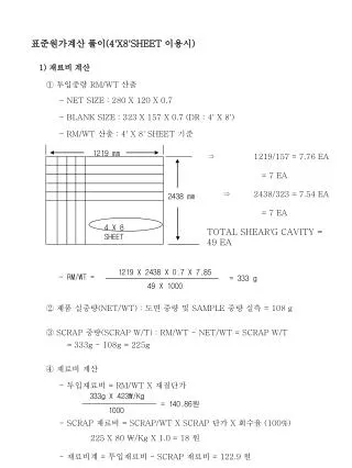
Download
1 / 24
250 likes | 391 Views
Sheet 4. Need to distinguish between: the address of a memory cell and the content of a memory cell Memory width ( m ): How many bits in each memory cell Address width ( n ): How many bits used to represent each address,

E N D
Need to distinguish between: • the address of a memory cell and the content of a memory cell • Memory width (m): • How many bits in each memory cell • Address width (n): • How many bits used to represent each address, • Determines the maximum memory size = address space using n, If address width is n-bits, then address space is 2n(0,1,...,2n-1)
Memory Width m bits Address width 0000000000000001 memory words 0 1 Address Space Or Memory Size 2 n 2 2n-1 Memory organization=2n x m
Q1 Given the following memory organization 1024 X 8 what is : • the number of address lines? • the number of data lines? • the memory size?
Q1 Given the following memory organization 1024 X 8 what is : the number of address lines? n = 10 1024 = 210 the number of data lines? m= 8 the memory size? =address space = 1024
Q 2 • A hypothetical machine with the following instruction format :
The particular I/O device identified within the 12-bit address Q2 • has the following instructions:
Q2 From the above structure, answer the following questions : • What is the maximum number of instruction set in this machine? • What is the address space available in this machine • What is the size of MAR,PC ? • What is the size of MBR, IR ?
m n bits M A R Memory Unit 2n x m Read / write data address Size of MAR = n Size of MBR = m MBR m bits Note : If a memory has k cells, they will have addresses 0 to k-1
Q2 From the above structure, answer the following questions : • What is the maximum number of instruction set in this machine? 2^4 = 16 • What is the address space available in this machine 2^12 = 4096 • What is the size of MAR,PC ? 12 bits • What is the size of MBR, IR ? 16 bits
Q 3 e. Fill out the following figure to explain the program execution and show the value of PC,AC,IR, MAR and MBR or I/O AR and I/O BR in each step of the following program: • Load AC from device 8. • Add contents of memory location 428. • Store AC to device 4. Assume that the next value retrieved from device 8 is 1 and the location 428 contains a value of 7.
CPU registers : • Program counter (PC) : address of instruction • Instructions register (IR) : instruction being executed • Accumulator (AC) : temporary storage • Memory Address Register (MAR): specifies the address in memory for the next read or write. • Memory Buffer Register (MBR): contains the data to be written into memory or receives the data read from memory. • Input /Output Address Register ( I/O AR ) : specifies a particular I/O device. • Input /Output Buffer Register (I/O BR) : is used for the exchange of data between an I/O module and the CPU.
Fetch Cycle • Program Counter (PC) holds address of next instruction to fetch • Processor fetches instruction from memory location pointed to by PC. • Instruction loaded into Instruction Register (IR) NOTE : this process involves the use of a memory address register (MAR) and a memory buffer register (MBR) • Increment PC • Unless told otherwise • Processor interprets instruction and performs required actions
Fetch Cycle • PC MAR • M[MAR]MBR • MBR IR • PC PC+1
Execute Cycle • Processor-memory data transfer between CPU and main memory • Processor I/O Data transfer between CPU and I/O module • Data processing Some arithmetic or logical operation on data . . .
Execute Cycle MAR = address part IF READ: M[MAR]MBR IF WRITE: MBRM[MAR].
Solution : (1) Determines an address in memory or I/O device
Solution (2) : Fill the memory contents • Operations: • Load AC from device 8. • Add contents of memory location 428. • Store AC to device 4.
Step 1 : Fetch ( Load AC from device 8 ) • Load AC from device 8. • Add contents of memory location 428. • Store AC to device 4. Memory CPU registers
Step 2: Execute ( Load AC from device 8) • Load AC from device 8. • Add contents of memory location 428. • Store AC to device 4. Memory CPU registers I/OAR=008 I/OBR=0001 AC 0001 Note : assume that the next value retrieved from device 8 is 1
Step 3: Fetch ( Add contents of memory location 428) • Load AC from device 8. • Add contents of memory location 428. • Store AC to device 4. Memory CPU registers • PC =301 (address of the first instruction ) • MAR=301 • M [MAR] MBR • M[301] MBR • MBR =4428
Step 4: Execute(Add contents of memory location 428) • Load AC from device 8. • Add contents of memory location 428. • Store AC to device 4. Memory CPU registers Read: MBR ← M [MAR] MAR=428 M[428] MBR MBR=0007
Step 5: Fetch (Store AC to device 4.) • Load AC from device 8. • Add contents of memory location 428. • Store AC to device 4. Memory CPU registers • PC =302 (address of the first instruction ) • MAR=302 • M [MAR] MBR • M[302] MBR • MBR =3004
Step 6: Execute (Store AC to device 4.) • Load AC from device 8. • Add contents of memory location 428. • Store AC to device 4. Memory CPU registers I/OAR=004 I/OBR=0008 AC 0008