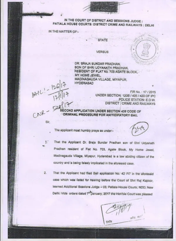
Download
1 / 52
520 likes | 595 Views
Understand the principles of Field Effect Transistors, including JFET and MOSFET, their parameters, biasing, switching, and applications. This guide covers SCR operation and characteristics as well.

E N D
Satish Pradhan Dnyanasadhana College, Thane ( Academic Year 2017 – 2018 ) SEM-VI T. Y. B. Sc. Electronics Unit 1 by Dr. S. R. Bhagat Dr. S. R. Bhagat
Field Effect Transistors • The current flow is controlled by electric field • Unipolar • Switch faster Dr. S. R. Bhagat
Field Effect Transistors • JFET MOSFET(IGFET) n-Channel JFET p-Channel JFET FET Enhancement MOSFET Depletion MOSFET n-Channel DMOSFET p-Channel DMOSFET n-Channel EMOSFET p-Channel EMOSFET Dr. S. R. Bhagat
FET and BJT • Unipolar Bipolar • High input resistance • No offset voltage • Immune to radiations • Less noisy • Greater thermal stability • Simple to fabricate less space Dr. S. R. Bhagat
Basic Ideas There are three terminals: Drain (D) and Source (S) are connected to n-cha Dr. S. R. Bhagat
Normal Biasing of JFET Dr. S. R. Bhagat
Drain Drain Drain Gate Gate Gate Source Source Source Schematic Symbols n-channel JFET Offset-gate symbol p-channel JFET n-channel JFET Dr. S. R. Bhagat
Drain Characteristics Dr. S. R. Bhagat
Drain Characteristics Dr. S. R. Bhagat
Transconductance Curve IDSS VGS (off)=VP Figure: Transfer (or Mutual) Characteristics of n-Channel JFET Dr. S. R. Bhagat
FET Parameters • Drain Resistance (rd) • The dynamic a.c. resistance is defined as the ratio of infinitesimal change in VDS to the corresponding change in drain current ID at a constant value of VGS • Transconductance (gm) • The mutual conductance is defined as the ratio of the change in drain current to the corresponding change in VGSat a constant value of VDS Dr. S. R. Bhagat
FET Parameters • The voltage amplification factor () • It is the ratio of change in VDS to the corresponding change in drain current VGS at a constant value of ID where Dr. S. R. Bhagat
Gate Bias Dr. S. R. Bhagat
Self Bias Dr. S. R. Bhagat
Voltage Divider Bias Dr. S. R. Bhagat
Common Source Amplifier Dr. S. R. Bhagat
JFET Analog Switch Dr. S. R. Bhagat
Shunt Switch Dr. S. R. Bhagat
Series Switch Dr. S. R. Bhagat
JFET Analog Switch Multiplexer Dr. S. R. Bhagat
FET as VVR Dr. S. R. Bhagat
Enhancement MOSFET Dr. S. R. Bhagat
Enhancement MOSFET Dr. S. R. Bhagat
Biasing of MOSFETDepletion Type Dr. S. R. Bhagat
Biasing of MOSFETEnhancement Type Dr. S. R. Bhagat
MOSFET Switch • The MOSFET switch is most popular type of switch. • It is good for transmitting low level voltage signals (as opposed to high current). • Output swing depends critically on RD (ID=IDSS for VGS=0). • Current flows at all times. Dr. S. R. Bhagat
A JFET has a drain current 5 mA. If IDSS = 10 mA and VGS(off) = 6V, find the value of VP and VGS • In a n-channel JFET potential divider biased circuit, it is desired to set the operating point at ID = 25 mA and VGS = 8 V. If VDD = 30 V, R1 = 1 M and R2 = 500 k, find the value of RS Given ] IDSS = 10 mA and VP = 5V • The transconductance of a JFET used in a voltage amplifier circuit is 3000 mho and the load resistance is 10 k , calculate the voltage amplification factor assuming that rd >> RL • For a JFET, IDSS = 9 mA and VP = 35V. Determine ID when VGS = 0 V and 2 V. Dr. S. R. Bhagat
A JFET amplifier employs voltage divider bias. The resistances are of value R1 = 1 M and R2 = 1 M. . If VDD is 20 V and the drain current is found to be 2 mA for RS = 15 k find VGS. If VDS is one half VDD, what is the value of RD? Dr. S. R. Bhagat
SCR Dr. S. R. Bhagat
Working of SCR • When Gate is open Dr. S. R. Bhagat
Working of SCR • When Gate voltage is zero Dr. S. R. Bhagat
Working of SCR • When Gate voltage is positive with respect to cathode Dr. S. R. Bhagat
Equivalent circuit of SCR • When Gate is open and V < VBr (Breakover voltage) • When gate voltage is positive Dr. S. R. Bhagat
Important terms for SCR • Forward Breakover Voltage (VBr) • It is the minimum forward voltage, gate being open, at which SCR start conducting heavily i.e. turned on. • Holding Current (IH) • It is the value of current below which the SCR switches from the conduction state to the forward blocking region under specified conditions • Peak Reverse Voltage (PRV) • It is the maximum reverse voltage that can be applied to an SCR without conducting in reverse direction Dr. S. R. Bhagat
Important terms for SCR • Forward Current Rating • It is maximum anode to cathode current that SCR is capable of passing without damage • Circuit Fusing Rating • It is the product of square of forward surge current and the time of duration of the surge Dr. S. R. Bhagat
V-I Characteristics of SCR Dr. S. R. Bhagat
SCR as a Switch • Advantages of SCR switch over mechanical or electromechanical switches • No moving parts, hence noiseless operation at high efficiency • The switching speed is very high upto 109 operations/sec • It allows control over large current upto 100 A in the load by means of small gate current • It is solid state device and has small size, hence gives trouble free long service Dr. S. R. Bhagat
SCR as a Switch • DC gate trigger • SCR turns on when switch S is closed Dr. S. R. Bhagat
SCR as a Switch • AC gate trigger • SCR turns on when IG IGT Dr. S. R. Bhagat
SCR as a Switch • Anode current interruption to make SCR off Dr. S. R. Bhagat
SCR as a Switch • Forced Communication Dr. S. R. Bhagat
SCR as a Half wave Rectifier Dr. S. R. Bhagat
SCR as a Half wave Rectifierwith firing angle upto 180 Dr. S. R. Bhagat
Triac Dr. S. R. Bhagat
TriacConstruction Dr. S. R. Bhagat
TriacOperation Dr. S. R. Bhagat
TriacCharacteristics Dr. S. R. Bhagat
Applications of TriacIntensity control of high power lamp Dr. S. R. Bhagat
Applications of TriacElectronic changeover of transformer taps Dr. S. R. Bhagat
The Diac Dr. S. R. Bhagat