Download
1 / 3
30 likes | 79 Views
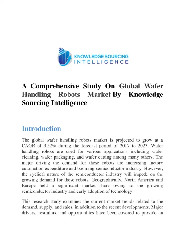
The demand for Wafer handling robots is increasing. The semiconductor industry is rising in such a way that it will drive the market over the upcoming years. Contact one of the experts at KensingtonLaboratories to know more in details.

E N D
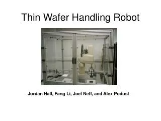
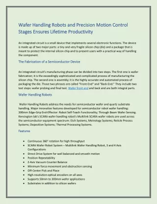
Wafer Handling Wafer Handling Robots and Precision Motion Control Robots and Precision Motion Control Stages Ensures Lifetime Productivity Stages Ensures Lifetime Productivity An integrated circuit is a small device that implements several electronic functions. The device is made up of two major parts: a tiny and very fragile silicon chip (die) and a package that is meant to protect the internal silicon chip and to present users with a practical way of handling the component. The Fabrication of a Semiconductor Device The Fabrication of a Semiconductor Device An integrated circuit's manufacturing phase can be divided into two steps. The first one is wafer fabrication; it is the exceedingly sophisticated and complicated process of manufacturing the silicon chip. The second one is assembly; it is the highly accurate and automated process of packaging the die. Those two phrases are called "Front-End" and "Back-End." They include two test steps: wafer probing and final test. Wafer front end and back end are both integral parts. Wafer Handling Robots Wafer Handling Robots Wafer Handling Robots address the needs for semiconductor wafer and quartz substrate handling. Major innovative features developed for semiconductor robot wafer handling: 300mm Edge-Grip End-Effector: Robot Self-Teach Functionality; Through Beam Wafer Sensing. Kensington lab's SCARA wafer handling robot's Multilink SCARA wafer robots are used across the semiconductor equipment spectrum: Etch Systems, Metrology Systems; Reticle Process Systems; Deposition Systems; Thermal Processing Systems. Features Features •Continuous 360° rotation for high throughput •SCARA Wafer Robot System – Multilink Wafer Handling Robot, 3 and 4 Axis Configurations •Direct Drive System for well balanced and smooth motion •Position Repeatability •Z-Axis Vacuum Counter Balance •Minimum force movement and obstruction sensing •Off-Center Pick and Place •High-resolution optical encoders on all axes •Supports 50mm to 300mm wafer applications •Substrates in addition to silicon wafers
•Through Beam Wafer Mapping •Position Self Teach Functionality •Single and Dual Arm configurations •No preventive maintenance (PM) requirements •Reliability – MCBF 10 million Cycles •Low-Cost-of-Ownership 300 mm FOUP 300 mm FOUP The FOUP is defined as Front Opening Universal Pod, which is the independent plastic enclosure implemented for handling the silicon wafers in a safe environment. FOUP is also called the Front Opening Unified Pod. The main purpose of this device is to designate the wafers in the machines to enhance the processing performance. 300mm FOUP was developed in the mid- 1990s as the wafer processing tool. Several companies design their FOUPs in several color combos, and the size of the product also varies according to the brand. Besides, IC processing equipment and the FOUP can prove advantageous in providing the nitrogen ecosystem to raise the productivity of the device. Earlier, the engineers could only develop the 300mm FOUP with the detachable cassette to place the wafer in the right position. But now, there are 400 mm wafer FOUP load ports that are also easily accessible from the robotics laboratory. It also allows the swapping of doors from front to bottom, which helps the robot mechanisms to access the wafer from the FOUP. Apart from that, the FOUP comprises many holes, pins, coupling plates that can be managed by the automatic material handling system and can locate over the load port. Advantages of Using the 300 mm FOUP Wafer Load Port Advantages of Using the 300 mm FOUP Wafer Load Port •The 300mm FOUP load port provides complete compatibility for all SEMI standard FOUPs. •The ROHS Compliant, SEMI Complaint, and CE certification ensure top-level performance. •There is no need for door & plate alignment with the 300mm FOUP. •The repeatable precision movements can be achieved with the DSP operated pneumatic closed-loop or electro-mechanical servos. •300mm FOUP comes with the bearings and lubrication-free screws. •The programmable lights, buttons, AMHS options, RFID, Barcode, OCR scanning, Class 1 cleanliness are some robust characteristics of 300mm FOUP.
Are you looking for 300mm FOUP load port wafer handling systems, the wafer handling robot applied material solutions, and precision motion control stages to maximize the life of equipment? Explore the Kensington Labs that have skillful engineers, who have extensive experience in wafer robot handling. Kensington aims to provide the most innovative, outstanding, and reliable wafer handling robots, ADOs, end-effectors, and aligners at the most affordable price. All the products come under warranty so that customers don't face any problem in case any issues occur. Source Link: https://bit.ly/3SWM89C