Download
1 / 3
30 likes | 39 Views
If one wishes to change one processed wafer with the unprocessed one, then intensifying the whole process of wafer front end becomes a real concern, demanding a whole lot of time. To abide by this rise in speed with precision and accuracy, these wafer handling

E N D
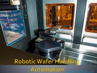
Wafer Handling for Robot Handling Industry The total productivity of the semiconductor industry is now turning out to be more dependent on the robotic handling industry. There is no denying in that too, and of course, it is all because of its functionalities and goods. If one wishes to change one processed wafer with the unprocessed one, then intensifying the whole process of wafer front end becomes a real concern, demanding a whole lot of time. To abide by this rise in speed with precision and accuracy, these wafer handling robots must always be driven at a better and quicker pace within the right mechanical coercion. Wafer Handling Robots These wafer handling robots are known to have the ability to depict all the needs and specifications for the semiconductors quartz, with ease and efficiency. These wafer handling robots and semiconductor robot handling altogether, do their work of beam wafer sensing, by not taking any extra time. These robots are extensively used for so many different processes like deposition systems, thermal processing systems, and many other more cases, in the semiconductor equipment spectrum. What is a wafer handling tool EFEM (Equipment Front End Module)?
Well, this is the tool that provides the highest safety in the wafer transfer process. With time, these wafers are not getting thinner than ever before, mainly because of the latest and inventive advances in the manufacturing process. As a result of this, it gets important to put up very thin and often strongly distorted wafers on post-process stages and at inspection times. Such wafer loaders have the ability to load ultra-thin wafers, having thinness of the littlest, with a great level of security and reliability that actually surpasses all the required demands of the semiconductor industry. Wafer front end functionalities and capabilities significantly reduce the wafer transfer time, which is actually the best part of it. Application of wafer handling tool EFEM (Equipment Front End Module) •Following are some of the major applications of EFEM: •For transfer stations and returns •For fully automated loading of frames and wafers from different cassettes •For external chucks •Adoption of different OEM tools to meet the customer needs deliberately
EFEM is configured to do the job of a wide range of semiconductor substrate processing. A business can integrate this sub-system with a professional’s assistance. There are so many other features too that one may have access to getting this tool deployed. Basically, it is configurable for different wafer- sized and substrate the right shapes while using the interface rightly. If you have any concerns and questions jiggling in your mind, feel free to contact the professionals of Kensignton Laboratories. They are really professional, having extensive expertise with them.Source Link: https://bit.ly/3geeXNI