Download
1 / 6
60 likes | 93 Views
The wafer stages program assists high-precision motion control in the nanometer variation for wafer positioning, testing, and alignment as practiced in Quality regulation and inspection.

E N D
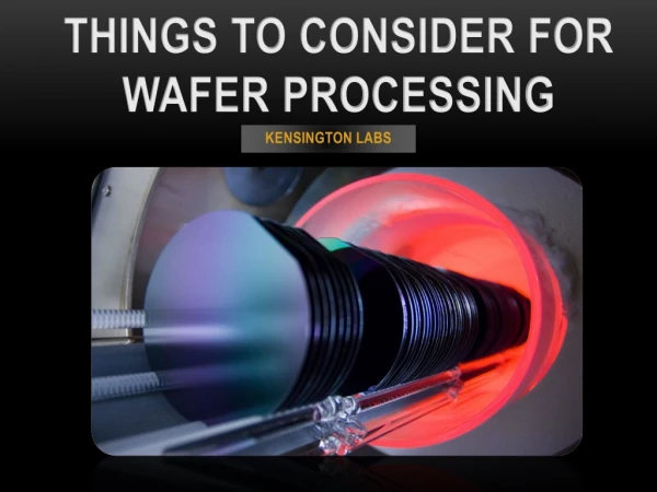
THINGS TO CONSIDER FOR WAFER PROCESSING KENSINGTON LABS
Introduction • The Wafer production technology necessitates extreme accuracy components, whether for wafer stages, imaging technologies or reticle stages. • The wafer stages program assists high-precision motion control in the nanometer variation for wafer positioning, testing, and alignment as practiced in Quality regulation and inspection.
Superiority Of Wafer • The Silicon Wafer Stage must abide by stringent conditions reliant on upon the task they are going to execute. • If you are comprised of a business that purchases wafers for the semiconductor market, there are several prominent deliberations that should always be the first priority in your list. • As with most merchandise, the price of silicon does oscillate relying upon external forces.
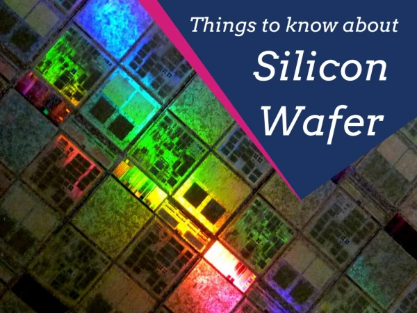
Types Of Wafer • There exists an abundance of various kinds of grades practiced to categorize wafers. • Ones that are bigger than fifty millimeters and one hundred are frequently circulated into mechanical test and process test diversities. • The latter is practiced chiefly for equipment created for testing and has importance on dimensional and structural features.
The procedure test wafer, at times entitled to as a monitor wafer, is the type utilized for precision motion control in the process of semiconductor process observing and fabrication, there exist additional wafer grades, comprising particle grade. • Further, Particle silicon wafers are mostly created to be used for the dimensions of actual elements.
Contact us https://www.kensingtonlabs.com/ service@kensingtonlabs.com https://twitter.com/kensingtonlabss 510.324.0126 https://www.linkedin.com/company/kensington-laboratories