Download
1 / 118
1.18k likes | 1.25k Views
This introduction covers types of data transmission, the difference between synchronous and asynchronous transmission, and specific protocols like SPI, I2C, and UART. Learn about data transmission for short and long distances, the advantages and disadvantages of synchronous and asynchronous transmission, techniques for handling errors, and characteristics of data words in serial communication.

E N D
Asynchronous and Synchronous Serial Communication COE 306: Introduction to Embedded Systems Dr. Aiman El-Maleh Computer Engineering Department College of Computer Sciences and Engineering King Fahd University of Petroleum and Minerals
Next . . . • Types of Data Transmission • Serial Transmission • Synchronous vs. Asynchronous Transmission • Serial Peripheral Interface (SPI) • Inter Integrated Circuit (I2C) • Universal Asynchronous Receiver Transmitter (UART)
Types of Data Transmission Serial Parallel Receiver Receiver 1 bit 1 word Transmitter Transmitter
Which of these Does not Send Data in a Serial Stream? USB Fiber Optic Cable Ethernet Parallel Port HDMI Serial Port
Which Type Should I Use? Serial Parallel Cost Speed Transmission Amount TransmissionLines TransmissionDistance Example Cheap Slow Single bit One line to transmit one to receive Long distance Modem Expensive Fast 8 bits (8 data lines) Transmitter & Receiver 8 lines for simultaneous transmission Short distance (synchronization) Printer Connection
Issues with Parallel Transmission • Inter-symbol interference (ISI) and noisecause corruption over long distances • If data is carried over multiple lines (parallel) it is possible that the data may arrive at different times at the receiver (skew); problem increases with higher frequencies • Bandwidth of parallel wires is much lower than bandwidth of serial wires • Parallel communication is faster than serial for short distances
Serial Transmission for Long Distances • Differential signals are used to increase power • Double the signal to noise ratio (SNR): it takes twice as much noise to cause an error with the differential system as with the single-ended system • Reach higher bitrate without noise • USB 2.0 is capable of 480Mbits/sec! 2Vs Vs Differential Signal
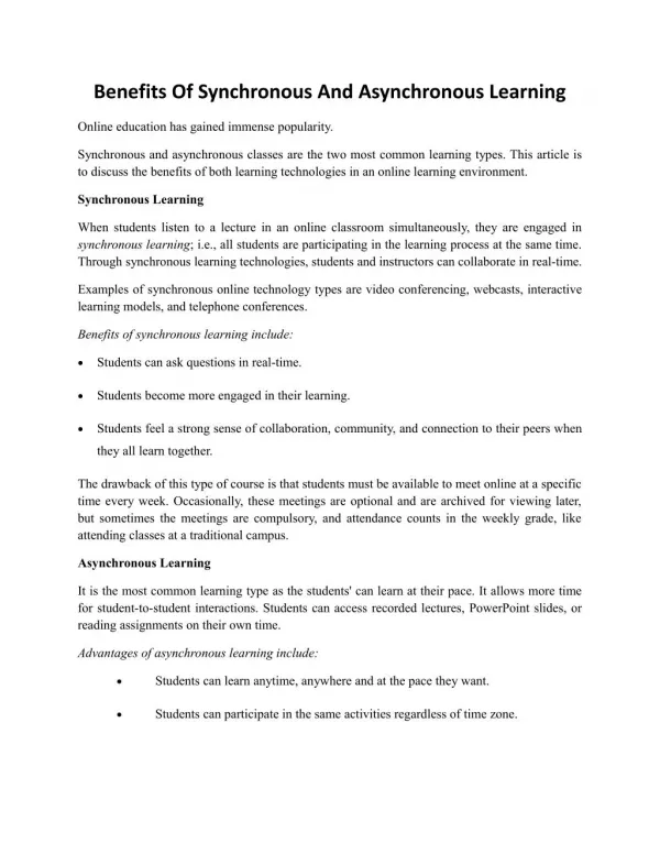
Synchronous vs. Asynchronous Transmission Synchronous Serial Transmission Asynchronous Serial Transmission • Data transmitted one character at a time • Each character contains its own clock • Start bits and stop bits • Resynchronizes with each character • Stream of data is encoded in chunks • Various bytes at the beginning of the data provide an embedded clock • The data stream can also be synchronized by an external clock
Synchronous Transmission Synchronous used for high-speed communication between computers Synchronous Serial Transmission • Advantages • Amount of overhead information restricted to few characters for each block • Can be used at higher speeds • Disadvantages • If error were to occur, whole block of data is lost (100+characters) • User cannot transmit characters instantaneously • Requires storage
Asynchronous Transmission Used for speeds up to 3000 bits/second with only simple single-character error detection • Advantages • Each character is its own complete timer system • Corruption will not spread • Good for irregular interval character generation • Keyboards • Disadvantages • Dependence on recognition of start bits • Many bits are used only for control purpose and carry no useful information • Limits transmission speed
Data Word and Control Bits Asynchronous Serial Transmission • Start Bit • Signals start of transmission of data bits • Transition from logic 1 to logic 0 • Data Bits • Typically 7 data bits (not including parity bit) • Least significant bit is transmitted and received first • Stop Bit • Signals end of data word = 1 • Parity Bit • Even or Odd; used for error detection
Example • Sending character ‘A’ with one start bit, one stop bit, evenparity, and 8 bit data • Binary Data is 0100 0001 • Parity Bit is 0 : as number of 1’s is even Parity Bit 0 0 1 0 0 0 0 0 1 0 1 Stop Bit Data Bits Start Bit Direction of Transmission
Simplex vs Duplex • Simplex • Data flow in only one direction • Such as from a PC to its peripheral • Full duplex • Data flow in both directions simultaneously • Such as a telephone conversation or communication via a modem • Half duplex • Data flow in both directions, only one direction at a time • Such as a conversation over a CB radio
BAUD Rates • Baud Rate: the rate at which symbols are sent • Measured in symbols per second (Bd) • Also known as baud or modulation rate • Often incorrectly referred to as bits per second • Important Baud Variables • Bd – Baud rate • M – Number of symbols used (voltages, tones, etc.) • Number of symbols used (M) = 2N where N = bits / symbol • N – Bits per symbol (binary = 1)
Bit Rates • Bit Rate: the rate at which bits are transmitted • Bit Rate = Baud * Bits / Symbol • Measured in bits per second (bps) NOT bytes per second (Bps) • Often incorrectly referred to as data rate • Gross Bit Rate – total number of bits transmitted per second • Includes protocol overhead bits and data bits • Rb = 1 / Tb where Tb is the bit transmission time • Symbol Rate ≤ Gross Bit Rate • Only equal when 1 bit per symbol (binary)
Bit Rates • Information Rate – rate at which useful data is transmitted • Information rate ≤ Gross Bit Rate • IR = Rb * Data Bit Number / Total Bit Number • Examples • Bit Rate • At 9,600 Baud with 4 voltage levels what is the bit rate? • Bit Rate= 9,600 * 2 = 19,200 bps • Information Rate • Given a protocol with 3 bits of protocol, 8 bits of data, 9600 baud, and 1 bit per symbol (binary) what is the IR? • IR = 9600 * 1 * 8/11 = 6981 data bits per second
Serial Transmission Interfaces • Synchronous • Serial Peripheral Interface (SPI) • Inter-Integrated Circuit(I²C) • Asynchronous • Universal Asynchronous Receiver Transmitter (UART)
Serial Peripheral Interface (SPI) • The Serial Peripheral Interface (SPI) bus is a 4-wire synchronous serial communication interface used for short distance communication • Developed by Motorola in the late eighties and has become a de factostandard • SPI devices communicate in full duplex mode using a master-slave architecture with a single master • Multiple slave devices are supported through selection with individual slave select (SS) lines
SPI Interface • The SPI bus specifies four logic signals: • SCLK : Serial Clock (output from master) • MOSI : Master Output, Slave Input (output from master) • MISO : Master Input, Slave Output (output from slave) • SS : Slave Select (active low, output from master)
SPI Operation • To begin communication, the bus master configures the clock, using a frequency supported by the slave device, typically up to a few MHz • The master then selects the slave device with a logic level 0 on the select line • During each SPI clock cycle, a full duplex data transmission occurs • The master sends a bit on the MOSI line and the slave reads it • The slave sends a bit on the MISO line and the master reads it • This sequence is maintained even when only one-directional data transfer is intended.
SPI Operation • Transmission involves two shift registers one in master and one in slave connected in a virtual ring topology • Data is usually shifted out with most-significant bit first, while shifting a new least-significant bit into same register • After register bits have been shifted out and in, master and slave have exchanged register values • If more data needs to be exchanged, the shift registers are reloaded and the process repeats • When complete, master stops toggling clock signal
SPI Clock Polarity and Phase • In addition to setting clock frequency, master must also configure clock polarity (CPOL) and phase(CPHA) • At CPOL=0 the base value of the clock is zero, i.e. the idle state is 0 and active state is 1 • For CPHA=0, data are captured on the clock's rising edge (low→high transition) and data is output on a falling edge (high→low clock transition) • For CPHA=1, data are captured on the clock's falling edge and data is output on a rising edge • At CPOL=1 the base value of the clock is one (inversion of CPOL=0), i.e. the idle state is 1 and active state is 0 • For CPHA=0, data are captured on clock's falling edge and data is output on a rising edge • For CPHA=1, data are captured on clock's rising edge and data is output on a falling edge
SPI Clock Polarity and Phase red vertical line represents CPHA=0; blue vertical line represents CPHA=1 CPHA=0 sampling on 1st clock edge; CPHA=1 sampling on 2nd clock edge
SPI Slave Configurations • Independent slave configuration • There is an independent chip select line for each slave • Slaves not selected should have high-impedance in MISO pins • Daisy chain configuration • Some products that implement SPI may be connected in a daisy chain configuration • The whole chain acts as a communication shift register • Can be used to propagate commands through a string of slaves; reduces HW cost
SPI Applications • SPI is used to talk to a variety of peripherals, such as • Sensors: temperature, pressure, touchscreens • Controldevices: audio codecs, digital potentiometers, DAC • Camera lenses: Canon EF lens mount • Memory: flash and EEPROM • Real-time clocks • LCD, sometimes even for managing image data • Any MMC or SD card
SPI Advantages • Full duplex communication • Higher throughput than I²C or SMBus • Complete protocol flexibility for the bits transferred • Extremely simple hardware interfacing • Uses only four pins on IC packages • At most one unique bus signal per device (chip select) • Not limited to any maximum clock speed, enabling potentially high speed • Simple software implementation
SPI Disadvantages • Requires more pins on IC packages than I²C • No hardware flow control by the slave (but the master can delay the next clock edge to slow the transfer rate) • No hardware slave acknowledgment (the master could be transmitting to nowhere and not know it) • Typically supports only one master device (depends on device's hardware implementation) • No error-checking protocol is defined • Only handles short distances compared to RS-232, RS-485, or CAN-bus
LPC176x/5x SPI Interface (SSP0/1) • The SSP is a Synchronous Serial Port (SSP) controller capable of operation on a SPI, 4-wire SSI, or Microwire bus. • It can interact with multiple masters and slaves on bus. • Only a single master and a single slave can communicate on the bus during a given data transfer. • Data transfers are in principle full duplex, with frames of 4 to 16 bits of data flowing from the master to the slave and from the slave to the master. • Maximum data bit rate of one eighth of the peripheral clock rate. • 8 frame FIFOs for both transmit and receive.
Clock Polarity (CPOL) and Phase (CPHA) control • When the CPOL clock polarity control bit is 0, it produces a steady state low value on the SCK pin. • If the CPOL clock polarity control bit is 1, a steady state high value is placed on the CLK pin when data is not being transferred. • The CPHA control bit selects the clock edge that captures data and allows it to change state. • When the CPHA phase control bit is 0, data is captured on the first clock edge transition. • If the CPHA clock phase control bit is 1, data is captured on the second clock edge transition.
SSPn Control Register 0 (SSP0CR0) LPC_SSP0 -> CR0 |= 0x0707; // 8-bit transfer; clk frequency divided by (7+1)
SSPn Control Register 1 (SSP0CR1) LPC_SSP0 -> CR1 |= (1 << 1); //SSP Enable
SSPn Data Register (SSP0DR) LPC_SSP0 -> DR=0; while ( (LPC_SSP0 -> SR & (1<<4)) ); data = LPC_SSP0->DR;
SSPn Clock Prescale Register (SSP0CPSR) • This register controls the factor by which the Prescaler divides the SSP peripheral clock SSP_PCLK to yield the prescaler clock that is, in turn, divided by the SCR factor in SSPnCR0, to determine the clock. LPC_SSP0 -> CPSR |= 0x5E; // slave dependent
SSP Initialization LPC_SC -> PCONP |= 1 << 21; //SSP0 interface power/clock control bit. LPC_SC -> PCLKSEL1 |= (1 << 10) | (1<<11); //Peripheral clock selection for SSP0. LPC_PINCON -> PINSEL0 |= 1 << 31; //Configure P0.15 to SPP0 CLK pin LPC_GPIO0 -> FIODIR |= 1 << 16; // Configure P0.16 to SSEL LPC_PINCON -> PINSEL1 |= 1 << 3; //Configure P0.17 to MISO0 LPC_PINCON -> PINSEL1 |= 1 << 5; //Configure P0.18 to MOSI0 //ENABLING PULL DOWN RESISTORS LPC_PINCON -> PINMODE0 |= 0x3 << 30; // P0.15 LPC_PINCON -> PINMODE1 |= (0x3) | (0x3 << 2) | (0x3<<4); // P0.16, P0.17, P0.18 LPC_SSP0 -> CR1 |= (1 << 1); //SSP Enable LPC_SSP0 -> CR0 |= 0x0707; // 8-bit transfer; clk frequency divided by (7+1) LPC_SSP0 -> CPSR |= 0x5E; // depends on the slave
Inter-Integrated Circuit (I2C) Bus • I²C (Inter-Integrated Circuit), is a multi-master, multi-slave, synchronousserial bus • invented in 1982 by Philips Semiconductor (now NXP Semiconductors) • Originally intended for operation on single board / PCB • Two wires carry information between a number of devices • One wire used for the data (SDA) • One wire used for the clock (SCL) • Half-Duplex; The speed grades (standard mode: 100 Kbit/s, full speed: 400 Kbit/s, fast mode: 1Mbit/s, high speed: 3.2Mbit/s). • Variety of devices are available with I2C Interfaces • Microcontroller, EEPROM, Real-Timer, interface chips, LCD driver, A/D converter
I2C Bus Characteristics • I²C uses only two bidirectional open-drain lines, Serial Data Line (SDA) and Serial Clock Line (SCL), pulled up with resistors • Unique start and stop condition • Slave selection protocol uses a 7-Bit slave address • The bus specification allows an extension to 10 bits • Acknowledgement after each transferred byte • No fixed length of transfer • Max. line capacitance of 400pF, approximately 4 meters (12 feet) • True multi-master capability: Clock synch., Arbitration
I2C Bus Definitions • Master • Initiates a transfer by generating start and stop conditions • Generates the clock • Transmits the slave address • Determines data transfer direction • Slave • Responds only when addressed • Timing is controlled by the clock line • Bus State • Quiescent (Idle), or in Master transmit mode or in Master receive mode
I2C Electrical Aspects • I2C devices are wire ANDedtogether • If any single node writes a zero, the entire line is zero
Bit Transfer on the I2C Bus • In normal data transfer, the data line only changes state when the clock is low SDA SCL Data line stable; Data valid Change of data allowed
SDA SDA SCL SCL Start Condition Stop Condition Start and Stop Conditions • A transition of the data line while the clock line is high is defined as either a start or a stop condition. • Startand Stopconditions are generated by bus master • The bus is considered busy after a start condition, until a stop condition occurs
I2C Addressing • Each node has a unique 7 (or 10) bit address • Peripherals often have fixed and programmable address portions • Addresses starting with 0000 or 1111 have special functions:- • 0000000 is a General Call Address (addresses all slaves) • 11110XX is 10-bit Slave Addressing 7-bit Addressing 10-bit Addressing
MSB LSB R / W ACK 7 – Bit Slave Address 1st Byte in Data Transfer on I2C Bus • Each node has a unique 7 (or 10) bit address R/W’ 0 – Slave written to by Master 1 – Slave read by Master ACK – Generated by the slave whose address has been output
Transmitter releases SDA line during 9th clock pulse. Acknowledgement from receiver Acknowledgements • Master/slave receivers pull data line low for one clock pulse after reception of a byte • Master receiver leaves data line high after receipt of the last byte requested
Transmitter releases SDA line during 9th clock pulse Not acknowledgement (NACK) from receiver Negative Acknowledge • NACK: Receiver leaves data line high for one clock pulse after reception of a byte • From Slave to Master Transmitter • After address not received correctly • After data byte not received correctly • Slave is not connected to the bus • From Master Receiver to Slave • After last data byte received correctly
Data Transfer on the I2C Bus • Start Condition • Slave address + R/W • Slave acknowledges with ACK • All data bytes • Each followed by ACK • Stop Condition
Data Formats • Master Writing to a Slave