Download
1 / 89
900 likes | 1.04k Views
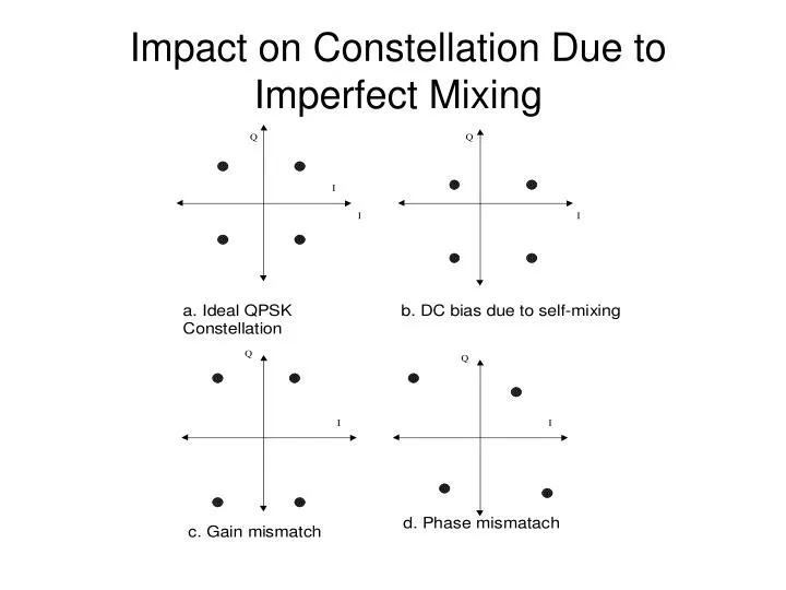
Impact on Constellation Due to Imperfect Mixing. Key Receiver Design Issues: AGC (1). Intermediate Frequency (IF) filter sets noise bandwidth of the Receiver Implementation impacted by cost, signal loss, and adjacent channel rejection. Key Receiver Design Issues: AGC (2).

E N D
Key Receiver Design Issues: AGC (1) • Intermediate Frequency (IF) filter sets noise bandwidth of the Receiver • Implementation impacted by cost, signal loss, and adjacent channel rejection
Key Receiver Design Issues: AGC (2) • Automatic Gain Control (AGC) • Placement for minimal noise (after IF for constant noise figure) • Large dynamic range to match the A/D dynamic range • Response time of AGC loop is critical for min. distortion and maximum dynamic range
Digital AGC To Software Receiver Input Signal A/D Converter Amp Gain Control Energy Detector Slew Gain Factor Mapping D/A Converter Inactive Mode Selector + Tracking - Reference Level
AGC Modes Reference Level Slew Mode Slew Mode Low amplitude level High amplitude level Input Signal Level Tracking Mode Tracking Mode AGC Inactive Zone
Key Transmitter RF Design Issues • Power Efficiency • Modulation Accuracy and Linearity • Spurious Signal Reduction • SNR of Transmitted Signal • Power Control Performance • Output Power Level
Transmitter Component Issues: Ocsillator & Mixer • Transmit IF VCO • noise floor • power consumption • phase noise provides significant modulation to narrowband signals • Up-Converter • Linearity to reduce spurious products • Noise floor • Power consumption
Key Transmitter Component Issues: Modulation • Modulator • balance between I&Q required to keep distortion (sidebands) down • Noise figure • Power consumption • Variable Gain Amplifier • Linearity and fidelity • Noise figure
Transmitter Component Issues: Transmit Filters • Transmit Filters • Isolation of transmitter noise from PA leaking into the receiver (supplement duplexer) • low loss required
Transmitter Component Issues: Power Amplifier (1) • Power Amplifier (very critical) • Cost - especially for base stations • Noise floor • Spurious response (source of interference)
Transmitter Component Issues: Power Amplifier (2) • Packing to handle heat • Low distortion traded for power efficiency traded for bandwidth (in practice only about 25% of the battery is effectively used during the talk time)
General Performance Metrics • Noise Characterization and Figure • Spurious Free Dynamic Range • Blocking Dynamic Range • Intermod • Power Consumption
Noise Characterization (1) • Noise is introduced into resistive components due to thermal actions. • where k is Boltzman’s constant (1.38.10-23 J/K), T is the temperature in Kelvin, R is component resistance (in ohms), and B is the bandwidth in Hz.
Noise Characterization (2) • Antenna is the first and the base line source of noise for which other noise sources are compared. • Thermal noise and quantization noise introduced by the A/D
Noise Figure • Noise Figure (NF) measure the amount of noise an element (or elements) adds to a signal. NF = SNRin/SNRout where SNRin is the input SNRout and is the device output SNR. • Active Components The manufacturer of a device usually supplies a noise figures for equals the loss of the passive components.
Using the Noise Figure (1/2) • It is possible to provide an equivalent system wide noise figure NFtotal that relates the noise back to the antenna. (equation 1) • Here NFi represents the noise figure at the ith stage and Gi represents the gain at the ith stage (units are linear).
Using Noise Figure (2/2) • Given a component with a noisy input having noise power Pi-1 (dBm), gain Gi (dB) and noise figure NFi (dB) the output noise power Pi(dBm)is given by Pi (dBm) = Pi-1 (dbm) + NFi(dB) + G (dB) Units are linear unless proceeded by (dB) or (dBm).
Example NF Calculations (1/2) NF3 =2 dB G3=10 dB NF2=2 dB G2=-2dB NF4=6 dB To Next IF Chain Cable, G1=-3dB From Anttenna BPF X LNA LO The total noise figure equals 5.975 .
Example Noise Calculations (2/2) Does ordering of the components yield optimal NF? • the total noise figure equals 3.6. • In the system, the LNA has the biggest impact on the noise figure (because of its high gain) • In general, it best to have higher gain components (like the LNA) located as early as possible in the RF chain. NF3 =2 dB G3=10 dB NF2=2 dB G2=-2dB NF4=6 dB To Next IF Chain Cable, G1=-3dB From Anttenna BPF X LNA LO
Calculating Sensitivity (1) • Sensitivity of the receiver to achieve a minimal signal-to-noise ratio SNRmin is defined as S dBm = Noise floor dBm + SNRmin dB where Noise floor dBm = 10 log (kTB) + NFtotal dB = 10 log(kT) dB + NFtotal dB + 10 log(B) dB and B is the end of system bandwidth and NF is the overall system noise figure.
Calculating Sensitivity (2) • For room temperature, the sensitivity becomes S dBm = -174 dBm/Hz + NF dB + 10 log(B) + SNRmin • A good conservative practice keeps the noise floor due to analog components lower than the noise introduced by the A/D converter.
Distortion Characterization: 1 dB Compression Point (1) • Devices that exhibit cubic characteristic, the third order distortion power grows at a rate of 3x the rate of the desired signal. • Eventually the device begins to saturate and when the actual output power level differs by 1 dB with the ideal output value, the 1 dB compression point P1dB is reached.
Distortion Characterization: 1 dB Compression Point (2) • Amplitude compression tends to block the detection of lower level signals in the presence of stronger signals and the blocking dynamic range (BDR)quantifies this effect. BDR = P1dB - MDS • The MDS level occurs when the input -signal is equal to the noise floor.
Output Power (dBm) P1dB,out 1dB Fundamental 1 1 Noise Floor MDS P1dB,in Input Power (dBm) BDR RF Distortion - BDR Output Power = G Input Power Output Power(dB) = Input Power(dB) + GdB MDS Minimum Detectable Signal P1dB,in Input 1 dB compression point P1dB,out Output 1 dB compression point BDR Blocking Dynamic Range BDR = P1dB,in - MDS
Spurious Free Dynamic Range (SFDR) Definition • The difference between the input levels for the MDS and the onset of third-order distortion (when the third order distortion equals the noise floor) defines SFDR.
SFDR Measurement (1) • The on-set of third-order distortion can be determined using the two-tone test, where two closely spaced tones of equal amplitude form the input to the system and the amplitude is increased until the third-order cross-product produces a signal equal to the noise floor.
Spurious Free Dynamic Range (2) • This test mimics real world situations where adjacent channel interference can cause significant intermodulation distortion. • Typical dynamic range values extend from 60dB to 90 dB.
3rd Order Intercept (IIP3) • IIP3 is found by extrapolating the fundamental and third-order intermod. product lines until they intersect. • The output power at this point is called the third-order intercept point (OIP3). • SFDR can be found from the two linear equations for the harmonic and third-order intermodulation product SFDR = 2/3 IIP3 – MDS
Output Power (dBm) OIP3 3rd Order IIM3 Fundamental 3 1 1 1 Noise Floor IIP3 MDS Input Power (dBm) SFDR RF Distortion - Intermod Predicts Susceptibility to Adjacent Channel / Nearby Interference IIP3 3rd Order Input Intercept Point OIP3 3rd Order Output Intercept Point SFDR Spurious Free Dynamic Range SFDR= 2/3 (IIP3 – MDS) IIM3 Intermod due to 3rd Order IIM3 = 3PI - 2 IIP3 (dBm)
System Level DistortionCharacterization • The effects of non-linear distortion are cumulative. An overall IIP (either IIP2 or IIP3), IIPtotal can be computed using the following approximation. where IIPi represents, in mW the Intermod Intercept Point (IIP) for stage i. • Like parallel resistors, the overall total is limited by the lowest value and the non-linearity at the later stages becomes more critical since its impact is magnified by the gain of all of the previous stages.
RF Distortion – Intermod for Cascaded Devices IIP3 =2 dB G3=10 dB IIP2=2 dB G2=-2dB IIP4=6 dB Cable, G1=-3dB From Antenna To Next IF Chain LNA BPF X LO “Dominated” by Worst IIPi
A/D Distortion Characterization • Composite RF and A/D noise and distortion is needed to quantify the overall receiver performance. • A conservative design approach is to choose an A/D converter that introduces insignificant noise contribution compared to the overall RF chain.
Example of A/D Impact • For instance, given an input noise at the antenna of –99 dBm, and a conversion gain of 25 dB and a noise figure of 10 dB, the input noise to the A/D is Ptotal = (-99dBm + 25dB + 10dB)= -64 dBm. • The percentage of noise power actually delivered to the A/D load from the RF front end can then be calculated. This noise voltage due to the analog components can be compared to the noise figure of the A/D converter. • A more precise analysis can determine the overall noise voltage by summing the effective voltage due to quantization with the voltage due to the analog components, VA/D,total = Vquant + VA/D,analog where Vquant = iA/D RA/D.
Example of A/D Impact (2) Ranalog + iA/D = Pquant / RA/D V A/D,total RA/D i analog = P analog,total / (R analog + RA/D ) - i analog = effective current from analog noise (RMS) iA/D = effective current due to A/D quantization noise P analog,total = noise power presented by the analog front end Pquant = quantization noise power Ranalog = equivalent analog resistance in series with A/D converter RA/D = resistance of the A/D converter
RF Distortion – Cascaded SFDR Cascaded SFDR Recipe • Determine Input Noise Power • Calculate System Gain • Calculate NFTotal • Calculate Output Noise Power • Calculate MDS • Calculate IIPTotal • Calculate SFDR
Using SDR to Change the “Cake Equation” • Software Radios have the added benefit of using both software and hardware which changes traditional tradeoffs • Examine two problems addressable by software radio: • PA nonlinearity vs efficiency • RF flexibility vs performance
Significance of the PA • Quality determines capacity • Output power defines coverage • Impacts size of BTS • Dominates infrastructure costs • Major contributor to BTS operating costs • Dominates power consumption
Transmitter Component Issues: Power Amplifier (1) • Power Amplifier (very critical) • Cost - especially for base stations • Noise floor • Spurious response (source of interference)
Transmitter Component Issues: Power Amplifier (2) • Packing to handle heat • Low distortion traded for power efficiency traded for bandwidth (in practice only about 25% of the battery is effectively used during the talk time)
8dB LOSS 4 x 20W SCPAs Combiners Handling Multiple Channels– Today’s Realizations SCPA – Single Carrier Power Amplifier MCPA – Multi Carrier Power Amplifier Antenna Radio Low power combiner Radio Band pass filter diplexer MCPA Radio MCPA based BTS GSM, GPRS & EDGE Radio
Realizing Multiple Channels with SDR and a Single PA Antenna Wideband digital radio Band pass filter diplexer MCPA Advantages over SCPA and Multiple Radio MCPA Most cost effective with multiple carriers More flexible More efficient Saves space Disadvantage: No redundancy and demanding PA specs
Summary of Cost Drivers in TX Design • Signal Peak-to-Average Power Ratio (PAR) • Signal Peak-to-Minimum Power Ratio (PMR) • Transmitter Power Control Dynamic Range (PCDR) • Signal Bandwidth • Transmitter Duplex Mode – half or full • Bandwidth Confinement Requirements (transmit mask) • Adjacent Channel Power (ACP, ACPR, ACLR) Earl McCuner, “SDR Radio Subsystems using Polar Modulation,” SDR Technical Conference, Nov. 11, 2002, pp. 23-27.
TX Requirements for Common Standards Earl McCuner, “SDR Radio Subsystems using Polar Modulation,” SDR Technical Conference, Nov. 11, 2002
Non-Linearity and Power Amps • Linearity • Class A – Best • Class AB, B – Mid-range • Class C – Worst • Efficiency • Class A – Worst • Class AB, B – Mid-range • Class C – Best
Memory Effects In PA (1/2) • High power, wideband amplifier characteristics exhibit hysteresis-like effects • Frequency-dependent electrical memory effects at high frequencies • Thermal memory effects at low frequencies • Linearization scheme must cancel the dynamic behavior of the PA
Predistortion with Memory Tapped Delay Line PD (TDL PD) Complex gain polynomial Hammerstein PD Filter
Memory Effects in PA (2/2) • 4-carrier W-CDMA input, PAPR = 13.7 dB • Class B power amplifier (30W approx.) hysteresis loops
Distortion Effects Non-Linearity >>> Spectral Regrowth Low PA Efficiency reduces battery life
Why is this a Problem? (1/2) • Modern comm. systems use non-constant envelope modulation • QAM • Non-Constant envelope signals require linear amplifiers • Changes in amplitude cause spurious emissions