Download
1 / 41
420 likes | 534 Views
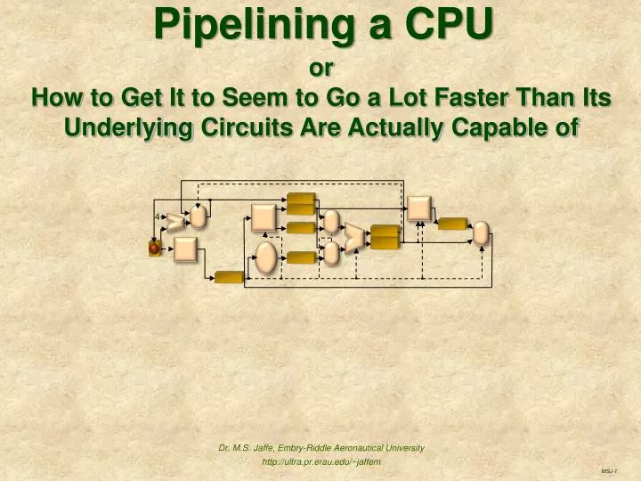
Pipelining a CPU. or How to Get It to Seem to Go a Lot Faster Than Its Underlying Circuits Are Actually Capable of. 4. Dr. M.S. Jaffe, Embry-Riddle Aeronautical University http://ultra.pr.erau.edu/~jaffem. The starting point: A typical CPU before pipelining

E N D
Pipelining a CPU orHow to Get It to Seem to Go a Lot Faster Than Its Underlying Circuits Are Actually Capable of 4 Dr. M.S. Jaffe, Embry-Riddle Aeronautical University http://ultra.pr.erau.edu/~jaffem
The starting point: A typical CPU before pipelining Instruction set architecture (ISA) Hardware architecture Instruction execution Asynchronous Synchronous (precursor to pipelining) After pipelining Hardware architecture Instruction execution Pipeline hazards and their solutions Short circuit logic Stall interlocks Summary Roadmap
The Instruction Set Architecture (ISA) of a CPU specifies the detailed behavior of each instruction the CPU can execute Assembly language is just a more readable form of machine language and some device drivers and other key parts of an operating system are still coded in assembly language, so hard core OS programmers must know the ISA of their machines Although a compiler need not be written in assembly language (horrors, what a thought!) a compiler writer will need to know a CPU’s ISA to write the compiler’s code generator Instruction Set Architecture
Your textbook chose the MIPS* to illustrate pipelining since it is a very simple CPU that’s what RISC means, right? Reduced Instruction Set Complexity The MIPS has a register-to-register architecture, a.k.a. load-and-store: Only the 2 instructions “Load” and “Store” can access memory under software control; all other operands for all other instructions come from CPU registers There are 64 basic operations (instructions) There are 32 software addressable, general purpose registers Example ISA: The MIPS * The MIPS is a commercial RISC architecture; for more information about it, see http://en.wikipedia.org/wiki/MIPS_architecture#Summary_of_R3000_instruction_set
R-type: Register-to-register, such as SUB R17,R5,R9 bit positions 0 5 6 1011 1516 2021 31 source register #1 (e.g. 5) source register #2 (e.g. 9) destinationregister (e.g. 17) opcode ALU function I-type: Immediate, such as ADDI R1,R3,-100 For an R-type instruction like SUB R17,R5,R9 (meaning R17=R5-R9), both operands are general purpose registers, as is the destination that stores the result, so the R-type instruction format must encode 3 register designations – and let’s just ignore the ALU function for the moment 0 5 6 1011 1516 31 bit positions • Since there are 64 possible operations, an instruction requires 6 bits to specify a unique operations code for each one (64 = 26, right?) • The 6 bit opcode is stored in bit positions 0 through 5; but don’t ask me why the textbook numbers the bits from the left rather than the right, which is more common • It takes 5 bits to uniquely specify a single general purpose register out of the 32 possibilities (0 through 31) • Here, for example, we see that for an R-type instruction, the destination register is specified by bits 16-20, which would be 100012, or 1710 for the example instruction SUB R17,R5,R9 source register #1 (e.g. 3) destinationregister (e.g. 1) immediate operand(e.g., -100) opcode J-type: Jump, such as Jump *-3560 0 5 6 31 bit positions immediate operand (offset to be added to program counter) opcode • For an I-type instruction, one operand is still a general purpose register, as is the destination, but the other operand is an immediate, a set of bits “immediately” available from within the instruction itself • Motivation: Compilers like to “conserve” general purpose registers; they’re valuable, and somehow we never seem to have enough of them. If the programmer writes, for example, x=y-100, why should we place the “100” in a memory location and then have to load in into a register before using it; it’s a constant and it’s never going to get changed by our code. Better to just compile it as a constant right into the instruction itself MIPS Instruction Format When we describe CPU operations, we’ll follow the textbook and designate the i’th general purpose register as Ri or occasionally as R[i] • All instructions are fixed length (4 bytes) • There are three instruction types (formats): • But for R-type instructions, the designer had to choose between: • Having separate opcodes for ADD and SUB, or • Requiring the program itself to explicitly complement a register before using ADDto perform a subtraction, the extra instruction thus increasing the length of the program • In other words, trading off an opcode against code density This example J-type instruction means, subtract 3560 from the PC and put the result back in the PC – such an instruction might appear at the end of a loop, when we want to jump backwards to the start of the loop • For a J-type, both the destination and one source register are implicit — the program counter • The other operand is an immediate Note that we’ll need a separate opcode to distinguish ADDI (add immediate) from an R-type ADD Also note that since immediate operands can be represented internally in 2’s complement, we don’t need a separate opcode for SUBI; ADDI can do both
Legend: The Hardware Architecture data control ? cond p1 p2 MUX 4 + NPC ALU p1 p2 MUX p1 p2 p1 p2 generalpurposeregisters A MUX MUX ALUoutput B Imm data.memory signextend LMD • The general purpose register set is a functional unit; it performs indexed storage and retrieval of data under software control i.e., machine language software gets to pick and choose which register will be used for what • We’ll sometimes use the R[i]notation, instead of just Ri, tohighlight the fact that the register set is an array of hardware registers whose contents are explicitly managed by a program’s software instruct.memory PC IR • Because of the tremendous disparity in speed between a modern CPU and large and cheap but comparatively slow main memories, the CPU must have a small but high speed (and hence more expensive) cache • The same basic CPU design could actually work directly with main memory here instead of cache, but it would be much slower; and a pipelined version of the CPU wouldn’t be worthwhile at all without the higher speed of a cache • The speed disparity between main memory and the CPU also dictates we cache data as well as instructions • Let’s leave until later in this course our discussion of the reason for having two separate caches — one for data and one for instructions, also called a “split” cache, or Harvard architecture — rather than a single, or “unified”, cache containing both • The CPU consists of: functional units that manipulate data (smart little thingies) special purpose registers (not visible to the software) that simply store and forward data between functional units (dumb little thingies) high speed cache We’ll review the workings of the CPU by stages, a stage being a set of related functional units and special purpose registers
Instruction Fetch ? cond p1 p2 MUX 4 + NPC +4 ALU p1 p2 MUX p1 p2 p1 p2 generalpurposeregisters A MUX MUX Meanwhile, since all instructions are fixed length, we can use a very small, special purpose adder to prepare the address for the eventual fetch of the next sequential instruction by just incrementing the PC ALUoutput But occasionally the current instruction we’re about to execute will (eventually) call for a jump or branch of some sort, so rather than simply sending the PC+4 value directly back into the PC, we’ll instead store it in the NPC (next program counter) and eventually send it into a multiplexer where we can, if need be, select an alternative – a branch or jump address computed later by the ALU – to be sent back to the PC instead B Imm data.memory signextend LMD instruct.memory PC IR C instruction fetch • After the instruction fetch, the CPU’s Instruction Register (IR) holds the instruction to be executed • The various bit fields of the instruction control all subsequent processing of this instruction by the CPU To get started executing that instruction, it must be fetched from instruction memory into the CPU ; so we send its address from the PC to the instruction memory to start the fetch At the start of an instruction execution, the Program Counter (PC) holds the address of the instruction to be executed
For register fetch, the IR6..10 and IR11..15 bits select which general purpose registers will be gated into the special purpose A and B registers • For example, if the instruction were SUB R3,R5, R1 (meaning R3=R5-R1)IR6..10 and IR11..15 would respectively contain the values 5 and 1 Instruction Decode and Register Fetch ? cond p1 p2 MUX 4 + NPC ALU p1 p2 MUX p1 p2 p1 p2 generalpurposeregisters A MUX MUX ALUoutput B Imm data.memory signextend LMD instruct.memory PC IR c c c c c c c Since the ALU for this particular machine (the MIPS) only accepts operands that are exactly 32 bits wide, we need a sign extension unit to left justify and then arithmetically right shift immediate operands from the IR to widen them to 32 bits for input to the ALU – inside of a 4 byte instruction, they couldn’t very well be a full 32 bits wide, now could they? instruction fetch instruction decode & register fetch Since I-type and J-type instructions use two different sizes of immediate operands, the sign extension unit needs to know the instruction type to correctly extract and widen the immediate operand After the register fetch, all four of the possible ALU operands have been fetched into special purpose registers, ready for the ALUinput multiplexers to select, based on the opcode, of course, the correct two to actually be input to the ALU After the instruction has been fetched into the IR, its various bit fields must be extracted, decoded, and sent to the functional units for use in the rest of the execution of this instruction
Execution or Address Calculation ? cond p1 p2 MUX 4 + c NPC ALU p1 p2 • For a branch instruction such as BZ R1,*-50, the designated register must be checked for the branch condition e.g., is R1 equal to zero? If so the condition register will be set to 1; otherwise it will be set to 0 • For a jump (unconditional), the condition register is set to 1 • Any other instruction sets the condition register to 0 MUX p1 p2 p1 p2 generalpurposeregisters A MUX MUX ALUoutput c B c Two multiplexers, under control of the opcode bits IR0..5, select which two of the four possible operands are actually sent to the ALU c c Imm data.memory signextend LMD c instruct.memory PC • The upper ALUinput multiplexer selects either NPC or register A as one input, depending on whether or not the instruction is a branch or jump — in which case a target address must be calculated based on the value of the NPC IR • The lower ALUinput multiplexer controls whether register B or the Imm is sent to the other ALU input port, depending on whether or not the opcode IR0..5 designates an R-type instruction instruction fetch instruction decode & register fetch execution or address calculation • For an I- or J-type instruction, the IR0..5 bits specify the operation to be performed by the ALU • For the more complex set of R-type instructions, the ALU function code in IR21..31 specifies the operation
Memory Access Depending on the current instruction type, ALUoutput could ultimately be used one of three different ways ? cond p1 p2 c MUX 4 + NPC ALU p1 p2 MUX p1 p2 p1 p2 generalpurposeregisters A MUX MUX Data memory will do one of three things, depending on IR0..5, the opcode of the instruction ALUoutput c The condition code controls what gets written back into the PC, i.e., either the NPC, or the target address for a branch or jump just calculated by the ALU B c c Imm data.memory • For a jump or branch instruction, e.g., JUMP *-3590, the ALU just calculated the address of the next instruction to be executed, which should (eventually) be sent to the program counter for the fetch of the next instruction signextend LMD • It could (eventually) be written back into a general purpose register, e.g., into R3 for an instruction like SUB R3, R5, R1, so the ALU just calculated R[5]-R[1] c instruct.memory PC • For a load, it will read from the address calculated by the ALU and place the contents at that address into the Load Memory Data register (LMD) • It could be used as the memory address for a load or store operation, e.g., LW R1,8(R2), meaningload word into R[1]from memory[R[2]+8], so the ALU just calculated R[2]+8 IR • For a store instruction, e.g., STW R7,96(R3), it will store special purpose register B which, for this example instruction, would contain the previously fetched contents of R[7] into the address, e.g., R[3]+96, just calculated by the ALU instruction fetch instruction decode & register fetch execution or address calculation memory access • For any instruction other than a load or store, data memory does nothing • The ALUoutput is sent to all three of the places where it might be used; each such downstream unit decides for itself whether or not it will actually use it
Write Back ? cond p1 p2 The specific register to be written to is designated by the destination register bits from the IR, e.g., the “17” in SUB R17, R5, R1, which is found in IR11..15 for an I-type instruction or IR16..20 for an R-type, the instruction type being obtained from IR0..5 MUX 4 + NPC ALU p1 p2 MUX p1 p2 p1 p2 generalpurposeregisters A MUX MUX ALUoutput B c c Imm data.memory signextend LMD instruct.memory PC IR instruction fetch instruction decode & register fetch execution or address calculation memory access write back write back • The opcode of the instruction determines whether it is the ALUoutput or the LMD that is written into some general purpose register • An R-type or any I-type instruction other than a load selects ALUoutput • A load instruction selects the LMD • A J-type doesn’t write back into the general purpose register set at all (only to the PC), so this multiplexer does nothing for a J-type instruction After the write back, instruction execution is complete and the PC contains the address of the next instruction to be fetched and executed
The starting point: A typical CPU before pipelining Instruction set architecture (ISA) Hardware architecture Instruction execution Asynchronous Synchronous (precursor to pipelining) After pipelining Hardware architecture Instruction execution Pipeline hazards and their solutions Short circuit logic Stall interlocks Summary Roadmap
Asynchronous Execution Time 400* ? cond p1 p2 MUX 1 + p1 p2 NPC MUX ALU A generalpurposeregisters p1 p2 MUX ALUoutput p1 p2 B MUX data.memory LMD signextend Imm PC instruct.memory IR 450 150 400 500 450 For this example, the length of the critical path, shown in orange, will be 2350 picoseconds so the instruction execution time is 2.35 ns • If the CPU is asynchronous, the instruction execution time is the time to execute the critical path through all the registers and functional units • I’ve made up some more or less totally arbitrary numbers; let’s assume they’re picoseconds * The write back has to use the general purpose registers set again, which, in this example, takes 400 picoseconds
Synchronous Operation instruction fetch instruction decode & register fetch execution or address calculation memory access write back 400* ? cond p1 p2 MUX 1 + p1 p2 NPC MUX ALU A generalpurposeregisters p1 p2 MUX ALUoutput p1 p2 B MUX data.memory LMD signextend Imm PC instruct.memory IR 450 150 400 500 450 • The critical path through the longest stage determines the minimum cycle time • In this example, then, we’d therefore need a cycle time of 550 picoseconds so that instruction decode and register fetch could complete in a single cycle The previous animations suggest an obvious partitioning into 5 stage-cycles To make the CPU synchronous, which is a necessary precursor to pipelining it, we’ll have to divide it up into a set of sequential stages, successive stages of which will start execution at the start of successive cycles
Synchronous Operation is Slower ? cond p1 p2 MUX 1 + p1 p2 NPC MUX ALU A generalpurposeregisters p1 p2 MUX ALUoutput p1 p2 B MUX data.memory LMD signextend Imm PC instruct.memory IR instruction fetch instruction decode & register fetch execution or address calculation memory access write back • The slowdown is the result of imbalance of our stage lengths • Since the cycle time was determined by the execution time of the longest stage, there is time “wasted” at the end of each cycle whose stage completes in less than the cycle time • The better balanced the stages are, the closer their critical path times are to the maximum one (the cycle time), the less time wasted per cycle in the shorter stages • It takes 5 cycles to complete an instruction • Since each cycle is 550 ps, it now takes 5 x 550 ps = 2.75 ns to execute an instruction, whereas an asynchronous execution only took 2.35 ns; we have slowed down our CPU’s performance by a factor of 2.75/2.35 1.17
Cutting the Pie Into Smaller Pieces May Not Help 400* ? cond p1 p2 MUX 1 + p1 p2 NPC MUX ALU A generalpurposeregisters p1 p2 MUX ALUoutput p1 p2 B MUX data.memory LMD signextend Imm PC instruct.memory IR instruct. decode instruction fetch execution or address calculation memory access write back register fetch 450 150 400 500 450 • The slowdown is the result of imbalance of our stage lengths • Since the cycle time was determined by the execution time of the longest stage, there is time “wasted” at the end of each cycle whose stage completes in less than the cycle time • The better balanced the stages are, the closer their critical path times are to the maximum one (the cycle time), the less time wasted per cycle in the shorter stages • Then the cycle time could drop from 550 to 500 ps (the time for the execution stage, which would have become the new “long pole in the tent”) • But since there would then be 6 cycles required to complete an instruction, the overall instruction execution time would go up to 6 x 500 ps = 3 ns; not what we wanted to achieve at all! Suppose we split instruction decode and register fetch into two separate stage-cycles?
Balance is the Issue ? cond p1 p2 MUX 1 + p1 p2 NPC MUX ALU A generalpurposeregisters p1 p2 MUX ALUoutput p1 p2 B MUX data.memory LMD signextend Imm PC instruct.memory IR instruction fetch instruction decode & register fetch execution or address calculation memory access write back • Remember this dilemma when we start to consider the depth of our pipeline: • Pipelining absolutely requires a synchronous design to start from • From the standpoint of the pipeline, the more distinct stage-cycles (which we will shortly start to call the “depth” of the pipeline), the better • But the more stages, the more difficult it may be to balance them • In reality, we’ll never be able to get our stages perfectly balanced, but the better balanced they are, the more efficient our synchronous design • As the number of stage-cycles increases, the difficulty of achieving a good balance among all the stages often increases as well and, as we saw, the overall execution time may actually go up
The starting point: A typical CPU before pipelining Instruction set architecture (ISA) Hardware architecture Instruction execution Asynchronous Synchronous (precursor to pipelining) After pipelining Hardware architecture Instruction execution Pipeline hazards and their solutions Short circuit logic Stall interlocks Summary Roadmap
execution/address calculation instruction decode/register fetch memory access instruction fetch write back instr. memory ⋮ ⋮ PC Overview of the 5 Cycle Synchronous CPU Processing Before Pipelining the 5 CPU stages • Let’s look at the sequencing as the CPU processes the 5 sequential instructions, instr.ithroughinstr.i+4, as shown to the left • Each instruction will take 5 cycles to work its way through the CPU instr. i instr. i+1 The CPU emitted a result (completed an instruction) every 5 cycles; so the 5 instructions took 25 cycles to complete instr. i+2 instr. i+3 instr. i+4
Pipelining exploits the fact that the various functional units of the CPU were actually idle most of the time A pipelined CPU overlaps the execution of several instructions simultaneously: During the same cycle, one stage can be working on one phase of one instruction while another stage can be working on a different phase of a different instruction – exactly like an assembly line Instructions advance through the pipeline from left to right in our diagrams ‒ earlier instructions are farther to the right, later instructions are farther to the left Needless to say, pipelining adds complexity to the CPU 4 E.g., the ALU was only active during 1 of the 5 cycles Pipelining writeback for instruction i instruction fetch forinstruction i+4 memory access byinstruction i+1 ALU execution byinstruction i+2 register fetch forinstruction i+3
the 5 CPU stages execution/address calculation instruction decode/register fetch memory access instruction fetch write back instr. memory ⋮ ⋮ PC Overview of the CPU Processing After Pipelining • Before pipelining, the CPU emitted an instruction every 5 cycles • Once the pipeline has been filled, the pipelined CPU can emit an instruction on every cycle • So eventually, after 5 cycles of “fill latency”, the CPU appears to be 5 times faster, despite the fact that each individual instruction still takes the same 5 cycles to work its way through the CPU • The speedup is equal to the number of stages that can work in parallel on different instructions, a.k.a. the depth of the pipeline instr. i instr. i+1 instr. i+2 instr. i+3 instr. i+4
the 5 CPU stages execution/address calculation instruction decode/register fetch memory access instruction fetch write back PC Details of the Pipelined Architecture and Its Operation instr. i+5 instr. i+4 instr. i+3 instr. i+2 instr. i+1 instr. i instr. memory At the end of the cycle: • All instructions will have advanced one stage to the right • instr.i will have been emitted (completed) • The PC will contain the address of instr.i+5 ⋮ ⋮ • We’ll look at the details of the cycle shown above, where the pipelined CPU is processing the 5 instructions ithroughi+4 in parallel • At the start of the cycle: • instr.i has been in the pipeline the longest and is on its 5th and final cycle, writing back its results into registers for other instructions to use in the future • The PC contains the address of instr.i+4, whose bits will be fetched into the CPU during this cycle instr. i+4 instr. i+5
instr. decode & register fetch for instr. i+3 execution or address calc. for instr.i+2 instr. fetch for instr. i+4 memory access for instr.i+1 write back for instr.i instr. decode & register fetch execution or address calc. instr. fetch memory access write back Similarly, all the initial data for a stage’s functional units must also come from the stage latches to their left, so … … are controlled by bits from the ID/EX.IR which, in this example, currently contains instr.i+2 instr. i+4 instr. i+3 instr. i+2 instr. i+1 instr. i • We’ll name the latches after the two stages of the pipeline they sit between • Here we see the IF/ID stage latches sitting between the Instruction Fetch and Instruction Decode stages • The IF/ID stage latches are the two registers now called IF/ID.NPC and IF/ID.IR IF/ID ID/EX EX/MEM MEM/WB ? cond p1 p2 MUX 4 + NPC NPC NPC ALU p1 p2 MUX p1 p2 p1 p2 generalpurposeregisters A MUX MUX Architecture of the Pipelined CPU ALUoutput ALUoutput B While the PC still controls the instruction fetch stage Not every stage needs every register – e.g., there’s no need for an ALUoutput latch in between the instruction fetch and instruction decode stages, since no functional unit involved in instruction fetch ever provided data to the ALUoutput register and no functional unit in the instruction decode or register fetch ever needed data from ALUoutput Imm data.memory B LMD signextend So, for example, the functional units of the execution/address calculation stage … instruct.memory PC IR IR IR IR • For this first cut at pipelining this CPU, the relationships among functional units will be almost completely unaffected; but we’ll have to make some changes later to fix some problems • The inner workings of the functional units themselves are completely unaffected with but a single exception that (almost) doesn’t even show at this level of architecture diagram, but it’s important (and expensive) nonetheless • The most visible change to the CPU architecture is that some of the special purpose registers must be replicated to complete a set of “pipeline registers”, a.k.a. pipeline latches or stage latches, that control each stage independently of the other stages • The stage latches sit between the adjacent stages of the CPU and mediate all data and controls moving from one stage to the next The functional units of a given stage are controlled by the Instruction Register (IR) immediately to their left … this is the configuration of the CPU at the start of the cycle Since we want the CPU to be working on multiple instructions in a single cycle like so: … we’ll need separate IR’s to hold the separate instructions that independently control each stage
After the write back of the results from instr.i(but still within the same cycle!), IF/ID.IR11..15 and IF/ID.IR16..20 identify the registers to be fetched into ID/EX.A and ID/EX.B for instr.i+3 to use during its execution phase on the next CPU cycle • Note that these control bits come from the IF/ID.IR, containing instr.i+3, not the MEM/WB.IR that controlled the prior write back for instr.i instr. i+4 instr. i+4 instr. i+3 instr. i+3 instr. i+2 instr. i+2 instr. i+1 instr. i+1 instr. i instr. i instr. i+5 instr. i+4 instr. i+3 instr. i+2 instr. i+1 IF/ID ID/EX EX/MEM MEM/WB As before, the target register for the write back is determined by bit fields within the instruction; but note that it isMEM/WB.IRcontrolling the write back, not IF/ID.IR ? cond p1 p2 c MUX 4 + NPC NPC NPC • Except that we have a problem, called a control hazard, with the PC, which we wanted to have come out set to the address of instr. i+5 but instead came out set to the address of instr. i+1 (oops) • Our first, very simple, pipeline contains a variety of hazards that we now need to investigate and fix +4 ALU p1 p2 MUX p1 p2 p1 p2 generalpurposeregisters A MUX MUX Operation of the Pipelined CPU ALUoutput ALUoutput c • With the exception of the general purpose registers, the functional units work exactly as they did before • Here, for example, for the write back of the results from instr.i, if MEM/WB.IR0..5 designates a load instruction, p2(containing MEM/WB.LMD) will be selected; otherwise the MEM/WB.ALUoutputat p1will be selected B Imm data.memory B LMD signextend instruct.memory PC IR IR IR IR c c c c c c c c c instr. decode & register fetch for instr. i+3 execution or address calc. for instr.i+2 instr. fetch for instr. i+4 memory access for instr.i+1 write back for instr.i At the end of the cycle: • The CPU has totally completed its processing of instructioni and emitted it • Instructions i+1throughi+4have each advanced one stage to the right • The CPU is ready for the next cycle, including the fetch of instruction i+5 At the start of a cycle, all the latches are gated out onto data and control lines to setup all subsequent processing for that cycle To complete the cycle, all current results are latched into the appropriate pipeline registers to set the stage for the next cycle
There are three sources of additional complexity so far (with more on the way ;-) More special purpose registers, now called pipeline latches, are required than for the un-pipelined CPU, since several of them have to be replicated to allow distinct sets of control and data to be provided to the distinct CPU stages to allow them to operate in parallel on distinct instructions The general purpose register set must be fast enough to be able to do both a write-back and a fetch in the same cycle, one after the other, the write-back first, so that the written back results from the earlier instruction, further down the pipeline to the right, are available as soon as possible for fetch into the pipeline registers ID/EX.A or ID/EX.B by a later instruction, further to the left, if required Extra control lines are need for the general purpose register set since it now does two independent operations each cycle and requires independent control for each Summary of Pipelining So Far
Our pipeline contains several hazards in addition to the control hazard with the PC; fixing these hazards will add further complexity Although the pipelined CPU, once filled, can emit an instruction every cycle, the cycle time itself may need to be increased to accommodate the extra delays through the extra stage latches and to allow the general purpose register set to complete two operations within the same cycle Summary of Pipelining So Far (cont’d)
The starting point: A typical CPU before pipelining Instruction set architecture (ISA) Hardware architecture Instruction execution Asynchronous Synchronous (precursor to pipelining) After pipelining Hardware architecture Instruction execution Pipeline hazards and their solutions Short circuit logic Stall interlocks Summary Roadmap
The design shown was deliberately over-simplified to show the basic concept of pipelined operations; it has several problems (a.k.a hazards) typical of pipelined designs that we will have to fix The cost of these fixes, obviously, will be even further complexity in the form of more circuits to make the pipeline work efficiently, including: Shortcut logic to resolve hazards without introducing stalls Interlocks for stall insertion for unavoidable hazards Let’s take a look at some of the hazards and the types of fixes the design will need Complications
IF/ID ID/EX EX/MEM MEM/WB ? cond p1 p2 MUX 4 + • The IF/ID.IR contains instr.i+3, R6=R3*R5, which, during the current cycle, will cause the values in R3 and R5 to be fetched and gated into the ID/EX.A and ID/EX.B stage latches so that they, the R3 and R5 values, can be sent to the ALU for the required multiplication on the next cycle, when instr.i+3 advances into execution • But the R3 value about to be fetched by instr.i+3is incorrect! NPC NPC NPC So the value about to be fetched from R3 by instr.i+3, is not the desired R2-R7value; it’s something left over from an earlier computation ALU p1 p2 MUX p1 p2 p1 p2 generalpurposeregisters A MUX MUX A RAW Hazard in the Pipeline The R2-R7 value we want instr.i+3 to fetch during this coming cycle from R3into ID/EX.B is not inR3; it hasn’t even been computed yet! ALUoutput ALUoutput B TheID/EX.IR contains instr.i+2, R3=R2-R7, which will cause the ALU to do the required subtraction this coming cycle Imm data.memory • Reminder: Its not R2 and R7 themselves being input to the ALU but ID/EX.A and ID/EX.B, which were set to R2 and R7 during the previous cycle, when instr.i+2 did its register fetch • We’ll still refer to the coming result as being the computation of R2-R7, however, since that’s what we’re really trying to achieve B LMD signextend • instr.i+3isn’t supposed to readR3 until afterinstr.i+2writes it • R3 is involved here in what is called a Read-After-Write (or RAW) data hazard, where the acronym reflects the order of operations desired but not obtained; the hazard is that we need a RAW but we won’t get it R2-R7 will be only computed by the ALU during this coming cycle, so it certainly can’t have been written back into R3 yet instruct.memory PC IR IR IR IR instr. decode & register fetch for instr. i+3 execution or address calc. for instr.i+2 instr. fetch for instr. i+4 memory access for instr.i+1 write back for instr.i • Suppose during this cycle our pipeline is processing, among others, the two instructions below: instruction i+2:R3=R2-R7 instruction i+3:R6=R3*R5
general purpose registers ALU p1 p2 p1 p2 MUX MUX p1 p2 p3 MUX “Shortcut” Logic Can Resolve This RAW Hazard The control logic for the expanded, lower ALUinput multiplexer also needs to be expanded, to allow it to recognize the hazard and select the EX/MEM.ALUoutput at port p3 rather than the (erroneous) ID/EX.B at port p2 whenever the hazard exists ― i.e., whenever the instructionin its execution cycle is an R-type instruction and one of its two source operand registers is the same as the immediately prior instruction’s destination register Here’s the expanded control logic for the lower ALUinput multiplexer that selects its new port p3 (containing EX/MEM.ALUoutput) whenever the hazard is detected: if (ID/EX.IR0..5 encodes an R-type opcode) and (ID/EX.IR6..10 == EX/MEM.IR16..20orID/EX.IR11..15 == EX/MEM.IR16..20), selectp3 else if ID/EX.IR0..5 encodes an I-type opcode, select p1 as usual (no hazard) else select p2 as usual (no hazard) This new logic is called “shortcut” logic, since the value in EX/MEM.ALUoutput takes a shortcut to get to the input port of the ALU when needed, earlier than when going through its regular writeback cycle Now, when all the pipeline registers are gated out at the start of the cycle, EX/MEM.ALUoutputand EX/MEM.IR are sent to the expanded lower ALUinput multiplexer which can recognize the hazard and select EX/MEM.ALUoutput vice ID/EX.B to resolve it when it occurs Note that at the start of the next cycle, after instr.i+3 has moved from register fetch into the execution stage, the R2-R7 result it needs will, in fact, now be available within the CPU, just not where it needs to be for instr.i+3 to use it, in ID/EX.B Note that the ALUoutput value must still be written back into the correct general purpose register so it is available “normally” as needed for future instructions execution for instr. i+3 ID/EX EX/MEM NPC B A ALUoutput Here’s the R2-R7 value we want instr.i+3 to work with, but it has not yet even been written back into R3, much less fetched into ID/EX.B where instr.i+3 needs it to be right now Imm The solution to the hazard is to add an additional port to the lower ALUinput multiplexer and connect EX/MEM.ALUoutputdirectly to it for selection in place of the erroneous ID/EX.B value whenever this hazard occurs IR c IR C C
p1 p2 p3 MUX Shortcuts Can Solve Many Problems But… • The previous slide showed the complexity incurred by one shortcut to resolve one hazard: • The multiplexer needs an extra port, which in turn requires a new data path to the new port • The control logic for the multiplexer gets more complicated, too, requiring yet more bits to be sent to it • Our simple pipeline has several other hazards; the good news is that many of them can be solved by shortcuts similar to the one we just saw • There are three pieces of bad news: • Because we’re adding additional circuitry to the CPU: • We may have to increase our cycle time a bit more • Our manufacturing cost per chip is rising since our yield is dropping with the increased area of each chip • There are still some hazards that can’t be resolved this way at all
In contrast to the RAW hazard we looked at previously, even after instr. i+3 moves into execution on the next CPU cycle, the data value it needs to be in R1 will still not be present anywhere in the CPU;it will still be being retrieved from data memory • So R1 is involved in a hazard that a shortcut can’t cure – the necessary data won’t be available to take a shortcut For Some Hazards, Shortcuts Won’t Work; Part of the Pipeline Must Be Stalled IF/ID ID/EX EX/MEM MEM/WB ? cond p1 p2 MUX 4 + NPC NPC NPC ALU p1 p2 MUX p1 p2 p1 p2 generalpurposeregisters A MUX MUX ALUoutput ALUoutput instr.i+2, which will ultimately load R1 with the value needed by instr.i+3, hasn’t even started reading the desired value from data memory yet; instr.i+2is still in address calculation, using the ALU to calculate the address Reg[2]+8 to send to data memory during its memory access on the next CPU cycle B Imm data.memory • During its decode and register fetch cycle, instr.i+3 needs to fetch the value from R1 and gate it into ID/EX.A for input to the ALU for the subtraction on the next cycle after instr.i+3 advances into execution • But the value we want for the subtraction is not inR1 yet, it’s still in data memory B LMD signextend instruct.memory PC IR IR IR IR instr. decode & register fetch for instr. i+3 execution or address calc. for instr.i+2 instr. fetch for instr. i+4 memory access for instr.i+1 write back for instr.i Inescapable conclusion: R4=R1-R5 must not be allowed to proceed into execution; the front (left) part of the pipeline must be stalled, its instructions prevented from advancing to the next stage to the right for the next cycle Suppose our instruction sequence includes the following instructions: instruction i+2: LW R1, 8(R2)meaning: load R[1] from memory[R[2]+8] instruction i+3: R4=R1-R5
execution/address calculation instruction decode/register fetch memory access instruction fetch write back Static View of the Stall the 5 CPU stages instr. i+4 instr. i+3 instr. i+2 instr. i+1 instr. i no-op no-op In general, whenever we stall an instruction that’s not ready to move on, we must also stall all subsequent instructions (which appear to the left in our diagrams) while allowing all preceding instructions (which appear to the right) to progress normally, so the hazard will eventually be cleared and it will be safe to let the stalled instruction move on again • But instr.i+2 must be allowed to proceed normally (without stalling), so that it will eventually read the correct data from data memory so that instr.i+3 can then proceed • And if instr.i+2 is to be allowed to proceed, instructions i+1andi must proceed as well so that they don’t get overwritten by the advancing instr.i+2 It is instr.i+3 that we really wish to keep from advancing But if we can’t let instr.i+3 advance, we have to hold up instr.i+4 as well, since there will be no place for it to advance to ― can’t have it overwrite instr.i+3, now can we ;-) instr. i+2: LW R1, 8(R2)[load R1 from memory[Reg[2]+8] instr. i+3: R4=R1-R5
no-op no-op execution/address calculation instruction decode/register fetch memory access instruction fetch write back Dynamic View of the Stall the 5 CPU stages instr. i+4 instr. i+3 instr. i+2 instr. i+1 instr. i • Although we held R4=R1-R5 in place after the last cycle, we still can’t let it advance after doing its register fetch (again!) on this cycle, since it will still be fetching a hazardous value: LW R1,8(R2) still hasn’t loaded the correct value into R1 yet • The correct value is still, in fact, not even in the CPU; this current cycle will fetch it from memory into the MEM/WB.LMD; it won’t be written back into R1 until the nextcycle when instr. i+2 does its writeback Now we can let R4=R1-R5 fetch (again) on this cycle and advance normally on the next, since the write back of MEM/WB.LMD into R1 will occur at the start of this current cycle just before R1is fetched into ID/EX.A We can’t let R4=R1-R5 move into execution after this cycle, since the value it is about to fetch from R1 is erroneous and a simple shortcut won’t resolve this hazard • Each stage that is inactive during a given cycle can be viewed as a stall “bubble” proceeding through the pipeline in place of a real instruction • Although it looks like we need a two cycle stall (two bubbles) here, we can cut that back to oneby simply adding a shortcut path from MEM/WB.LMD to the upper ALUinput multiplexer so that we don’t actually have to wait for the write back of the correct value into R1
no-op no-op execution/address calculation instruction decode/register fetch memory access instruction fetch write back Using a Shortcut to Reduce the Number of Stall Bubbles the 5 CPU stages instr. i+4 instr. i+3 no-op instr. i+2 instr. i+1 instr. i+5 • We can let instr.i+3 advance into execution here, after only a one cycle stall, not two, since at the start of this cycle, the data from MEM/WB.LMD can take a shortcut to an expanded upper ALUinput multiplexer which can detect the hazard and select the MEM/WB.LMD value instead of the hazardousID/EX.A it would normally gate into the ALU for execution • Now instr.i+3can execute normally with no problem • Note that on this cycle, the memory access stage must execute a no-op since the execution stage, having executed a no-op on the previous cycle, produced no results for use by the memory access stage during this coming cycle • The stall bubble has propagated — advanced in the pipeline in place of a normal instruction At the end of this cycle (with a stalled execution stage), the data needed for instr.i+3’s execution has been retrieved by from data memory by instr.i+2’s memory access and placed in MEM/WB.LMD for writeback into R1 on the next cycle During this cycle, instr.i+2 performs its memory access and sets MEM/WB.LMD to the desired value Note that instr.i+2 must still perform its normal writeback so that R1 will be correctly set for other instructions to use in the future
4 C C C C C C C C Pipeline Interlocks Are Required to Insert the Stall Bubble All four interlock multiplexers have the same control logic: If the ID/EX.IR contains a load instruction whose destination register is the same as a source register for the instruction in the IF/ID.IR, then select port p1 (stall), else select port p2 (normal) • We’ll need 4 new multiplexers in the front-end stage latches • To stall i+4 and i+3, the PC, IF/ID.NPC, and IF/ID.IR registers must recycle their current contents (leave them in place and not send them to the next stage) to ensure that execution can resume normally once the hazard is cleared • Additionally, the ID/EX.IR must be set to all zeroes (no-op) to insert the stall bubble into the next stage for the next cycle EX/MEM.ALUoutput EX/MEM.cond IF/ID ID/EX p1 p2 p1 p2 MUX MUX NPC Legend: p1 p2 MUX stall + p1 p2 MUX p1 p2 p1 p2 MUX MUX 0 normal IR PC IR C instr. memory C C C C C C
p1 p2 MUX ADD Legend: 4 4 stall p1 p2 MUX normal C C Stalling the Front End Here’s how instr.i+2 and instr.i+3 get recycled (stalled in place) and a stall bubble (no-op) inserted into the pipeline’s execution stage in place of the stalled instr.i+3 Up to this point, everything has been proceeding normally, but since the opcode for instr. i+2, LW R1, 8(R2), specifies a load and its destination register matches one of the source registers for instr. i+3, R4=R1-R5, all the interlocks will now select port p1, which will stall (recycle) the first 2 stages of the pipeline on the next cycle as well as inserting a no-op stall bubble into the 3rd stage We won’t showthe execution/address calculation, memory access, or write back stages this cyclesince they’re all operating normally, which we’ve already seen Since the ID/EX.IR controls the execution stage and it’s about to be set to all zeroes (the code for “no operation”) for the next cycle, it actually doesn’t matter what’s about to be gated into the other ID/EX registers at the end of this cycle; the no-op on the next cycle means thatthey won’t be used anyway so we won’t bother to show them here Since we don’t care about any of the ID/EX registers except the IR, the instruction decode/register fetch stage functional units that feed those other ID/EX registers also don’t matter in this animation; although they’re not really stalled, their outputs are just going to be ignored anyway; so to keep the animation as simple as possible, we won’t show their processing this cycle either At this point, the PC, IF/ID.IR, and IF/ID.NPC are set to recycle – the contents about to be gated in are the same as they were at the start of the cycle, so instr. i+4 and instr. i+3 will not advance in the pipeline OK, enough caveats; here we go ;-) The stall insertion is complete; PC, IF/ID.IR, and IF/ID.NPC have been recycled and ID/EX.IR is set to no-op (all zeroes) Additionally, since instr.i+3 is being stalled in place and the execution stage will hence have nothing to do on the next cycle, a no-op will be gated into the ID/EX.IR so that the execution stage functional units, controlled as they are by the ID/EX.IR, will in fact do nothing EX/MEM.ALUoutput c EX/MEM.cond IF/ID ID/EX ID/EX p1 p2 p1 p2 MUX MUX NPC +4 p1 p2 p1 p2 MUX MUX 0 0 IR PC IR C C C C instr. memory C C C C C C C C C
execution/address calculation instruction decode/register fetch memory access p1 p2 MUX instruction fetch write back ADD Legend: 4 4 stall p1 p2 MUX normal C C Purging the Stall Bubble • Here’s the stall bubble • Normal operations of the CPU will eliminate it in 3 more cycles instr. i+5 instr. i+4 instr. i+3 no-op instr. i+2 instr. i+1 instr. i+6 instr. i+7 instr. i+8 EX/MEM.ALUoutput EX/MEM.cond • After three cycles, the stall bubble has been expelled • Note that although it took 3 cycles to clear the bubble, in only one of those 3 cycles (the last one, when the bubble itself was emitted) did the CPU not emit an actual result (i.e., complete an instruction); so the loss of efficiency is proportional just to the number of stall bubbles inserted (just 1, in this case), not the number of cycles (3) during which that bubble was present somewhere in the pipeline IF/ID ID/EX ID/EX p1 p2 p1 p2 MUX MUX NPC p1 p2 p1 p2 MUX MUX 0 IR PC IR instr. memory
Examination of the “normal” advance of the PC into the NPC in the previous animation reveals that it is unfortunately incorrect The reason actually has nothing to do with the interlocks but resulted from the earlier introduction of the extra pipeline registers for the NPC themselves; the NPC logic was correct in the un-pipelined design And things are really going to go to worms when we add jump and branch instructions rather than just the simple sequential execution we’ve been looking at ― we may already have fetched and decoded an instruction we actually don’t want to execute at all; ugh! But I’ll leave animating the fixes for those issues for another year (read the textbook ;-) Next Complication: The PC, the NPC, and Branch Hazards
The starting point: A typical CPU before pipelining Instruction set architecture (ISA) Hardware architecture Instruction execution Asynchronous Synchronous (precursor to pipelining) After pipelining Hardware architecture Instruction execution Pipeline hazards and their solutions Short circuit logic Stall interlocks Summary Roadmap
Despite the fact that the underlying circuitry is no faster than before, an n-stage pipeline emitting 1 result per cycle* gives the appearance of an n-fold speedup In actuality, the speedup is less than that for two reasons: The cycle time itself may need to increase to allow for extra propagation delays through the new circuits (e.g., stage latches) Some cycles will not see an instruction completed and emitted: For a pipeline with n stages, n cycles of “pipeline latency” are required to fill the pipeline before instructions start to complete; jumps and branches may cause this penalty to occur repeatedly There will almost always be hazards that shortcuts can’t cure so the front end of the pipeline will have to be stalled; each stall bubble inserted eventually leads to a cycle where no instruction completes Summary * Some (currently irrelevant) jargon: A CPU that emits 1 result per cycle is said to be “base scalar”