Download
1 / 25
260 likes | 388 Views
Explore the world of line defects like dislocations – their movement, impact on deformation, and creation of defects in materials. Uncover insights on slip, stress fields, and planar defects inflicted by dislocations and grain boundaries.

E N D
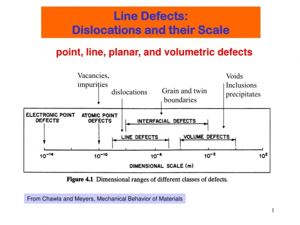
Length Scale of Imperfections Line Defects: Dislocations and their Scale point, line, planar, and volumetric defects Vacancies, impurities Voids Inclusions precipitates Grain and twin boundaries dislocations From Chawla and Meyers, Mechanical Behavior of Materials
Line Defects: Dislocations Dislocations: • are line defects, • cause slip between crystal plane when they move, • produce permanent (plastic) deformation. Schematic of a Zinc (HCP): • before deformation • after tensile elongation slip steps Adapted from Fig. 7.9, Callister 6e. Actual strained hcp Zn
Incremental Slip and Bond Breaking • • Dislocations slip planes incrementally... • Dislocation motion requires the successive bumping • of a half plane of atoms (from left to right here). • • Bonds across the slipping planes are broken and • remade in succession. Atomic view of edge dislocation motion from left to right as a crystal is sheared. Shear stress Snapshot midway in shear (Courtesy P.M. Anderson)
EdgeDislocations Exiting Crystal Form Steps Burger’s Vector = b Shear stress The caterpillar or rug-moving analogy
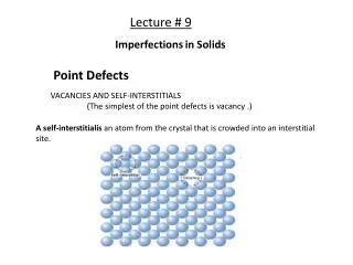
Dislocations are line defects that separate Slipped vs Not Slipped. • They form loops inside crystal, having screw, edge and mixed character. • Dislocation moves perpendicular to line direction along each segment. • Top of crystal moves in direction of b (Burger’s vector). • Same surface steps created. Hayden, Moffatt, Wulff, “The Structure and Properties of Materials,” Vol III (1965)
Formation of Steps from Screw and Edge Dislocations Shear stress Edge Shear stress Screw Both screw and edge motion create same steps!
The EdgeDislocations and Burger’s Vector Looking along line direction of edge Burger’s vector = extra step • Edge looks like extra plane of atoms. • Burger’s vector is perpendicular to line. • Positive Edge (upper half plane) • Is there a Negative Edge? • Where is it? • What happens when edge gets to • surface of crystal? • What are the stresses near edge? • Like trying to zip up those old jeans. Stress fields at an Edge dislocation
Burger’s vectors mostly on the most close-packed planes in the most closed-packed direction What are the most close-packed PLANES AND DIRECTIONS fcc, bcc, and sc? b
Almost complete plane of atoms Slip plane Non-overlapping vacancies Slip plane Slip plane Overalapping Extra atoms go into interstitial Slip plane Dislocations Can Create Vacancies and Interstitials • All defects cost energy (J/m2 or erg/cm2) • But getting rid of defects, like large dislocations, does lower energy (but not to perfect crystal). • Dislocations can annihilate one another! • Non-overlapping edges create vacancies. • Overlapping edges create interstitials.
Planar Defects: Surfaces • All defects cost energy (energy is higher than perfect crystal) • Surfaces, grain, interphase and twin boundaries, stacking faults • Planar Defect Energy is Energy per Unit Area (J/m2 or erg/cm2) • Surfaces: missing or fewer number of optimal or preferred bonds. surface
Grain boundaries high-angle surface low-angle Planar Defects: Grain Boundary • All defects cost Energy per Unit Area (J/m2 or erg/cm2) • Grain boundary: fewer and/or missing optimal bonds. • - low-angle GB and high-angle GB.
Relative Energies of Grain Boundaries high-angle Grain I • The grains affect properties • mechanical, • electrical, … • Recall they affect diffraction so you know they’re there. • What should happen to grains • as temperature increases? • Hint: • surfaces (interfaces) cost energy. Grain 2 Grain 3 low-angle
Tilt Twist Bi-crystals are made by twist boundaries Dislocation Interactions Can Create Planar Defects! Small-Angle Grain Boundaries: a tilt and a twist b • All defects cost energy (J/m2 or erg/cm2) • Tilt Grain boundary: • - from array of edge dislocations • - misorientation of crystal planes = • Twist Grain boundary • - when is parallel to boundary • Should energy of GB depend on? • If dislocation cost energy, how are they there? C T d sin~ =b/d
original atomic positions before twinning Twin Boundaries: an atomic mirror plane • There has to be another opposite twin nearby to get back to perfect crystal, • becauseall defects cost energy (J/m2 or erg/cm2) and to much defect costly. • Stress twins can be created (e.g., Tin) in which case the atoms must move • at the speed of sound. • What happens when something moves at speed of sound?
f Cu-8.0at.%Al Sudden load drop accompanies twinning q fcc normal twinning direction twin fcc twin plane F Schmid factor M. S. Szczerba, T. Bajor, T. Tokarski Phil. Mag. 84 (2004) 481-502. Twin Boundaries: Load drop in F vs %EL Stress twins are created and work to create them lead to load drop.
hcp ...ABCACABABCABC... …….fcc fcc ……….. Stacking Faults: Messed up stacking FCC HCP or C slip or C • All defects cost energy (J/m2 or erg/cm2). • Stress, dislocation motion can create Stacking Faults. • What is stacking of FCC and HCP in terms of A,B, and C positions in (111) planes? …ABCABCABC…
Optical Microscopy • Useful up to 2000X magnification. • Polishing removes surface features (e.g., scratches) • Etching changes reflectance, depending on crystal orientation. close-packed planes Adapted from Fig. 4.11(b) and (c), Callister 6e. (Fig. 4.11(c) is courtesy of J.E. Burke, General Electric Co. micrograph of Brass (Cu and Zn) 0.75mm
Optical Microscopy Grain boundaries... • are imperfections, • are more susceptible to etching, • may be revealed as dark lines, • change direction in a polycrystal. Adapted from Fig. 4.12(a) and (b), Callister 6e. (Fig. 4.12(b) is courtesy of L.C. Smith and C. Brady, the National Bureau of Standards, Washington, DC [now the National Institute of Standards and Technology, Gaithersburg, MD].)
Polymer, too: Colloidal Epitaxy via Focused Ion Beam Lithography Silica (f=1.18mm, 0.5vol%) Zirconia (f~ 3nm, 0.03vol%) SEM of patterned cover slip From Prof. Braun’s group. On cover of Langmuir (2004) Sedimented growth: dislocations and SF In 37th layer: GB and SF Objective lens
Use Microscopy to see defects: contrast using optical, electron, scanning probe Poly-xtal Pb ~1x • Optical ~ 2x10³ x • Scanning EM ~ 5x10⁴ x • High-resolution TEM ~106 x • Scanning probe ~109 x topo-map) Poly-xtal Cu-Zn 60x Fe-Cr GB 100x Dislocation in Ti alloy ~50,000 x Old brass door knobs have been etched by acid in your sweat and you can see with your eyes the grains and their different orientations. Move w/ and change w/ T
In focus TEM Image of Dislocations in Ti Alloy • Why are dislocations not loops? • Dislocations are formed • -solidification • - plastic deformation • - thermal stresses from cooling 51,450 x
SUMMARY • Defect materials responsible for most desired properties useful to engineering, e.g., mechanical, thermal, and electrical. • They occur in metals, ceramics, polymers, and semiconductors. • Defect can be categorized in terms of Point, Line, or Planar defects. • Point: vacancies, interstitials, substitutional, … • Line: dislocations (mostly for metals, but not exclusively). • Planar: surfaces, grain boundaries, boundaries (twin, antiphase, domain, tilt … ), stacking faults, … • Defects can be observed by eye or various microscopies. • Defects can be created or affected by temperature, stress, etc., requiring or leading to other defects, as with dislocations.