Download

1 / 15
150 likes | 325 Views
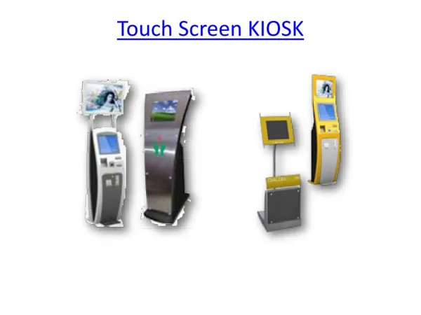
SAM9RL Touch Screen ADC Controller. Introduction to Resistive Touch panel. Resistive touch panel technology is the most common, due to its simplicity and low cost characteristics.

E N D
Introduction to Resistive Touch panel • Resistive touch panel technology is the most common, due to its simplicity and low cost characteristics. • It can be found in PDAs, Mini Notebook, Phone, Medical Equipment, Office Automation, Consumer Products, POS, information servers, … • Analogue resistive technology can be separated into 4-wire, 5-wire, 6-wire, 7-wire, and 8-wire according to screen size. • The most popular are 4-wire and 5-wire systems • The SAM9RL64 TSADC is dedicated to 4-wire resistive touch panel ( >15’’ diagonal can be found)
6 Touch Screen ADC Controller: Block Diagram • Based on a 10-Bit SAR ADC • ADVREF range from 2.6V to VDDANA. • Up to 6 analog lines with 4 touch screen channels (can be used as normal ADC) • 4 power switches measuring both axis (X,Y) on resistive touch screen panel • Pen Detect and Pen Loss interrupt • Trigger Mode: External Trigger, Continuous, Periodic, Pen detect
Resistive Touch screen Principle Polyester Film Conductive ITO (Transparent Metal Coating) Upper Resistive Circuit Layer Lower Resistive Circuit Layer Insulating Dots Glass - Substrate A press causes the Upper Resistive Circuit Layer to contact the Lower Resistive Circuit Layer, producing a circuit switch from the activated area.
The 4-Wire Resistive TS Structure PEN contact Voltage Measurement X Position VDD VDD = 3V X+ X- GND VY+ = 1.5V Y- Y+ Glass GND = 0V The ratio of this measured voltage to the drive voltage applied is equal to the ratio of the x coordinate to the width of the touch screen. => x = ½ width of touch screen
TSADCC: Position Measurement • To detect the position of a contact: • Supply voltage is applied between Xp and Xm • Voltage measured on Yp • Supply voltage is applied between Yp and Ym • Voltage measured on Xp • The position is defined by [ (VYp / VDD) , (VXp / VDD) ]
TSADCC: Position Measurement • The switches added to control the power supply are resistive: • High voltage reference is not VDDANA • Low Voltage reference is not GND • Compensation of switches loss is necessary : • [ X , Y ] • [ (VYp – VXm) / (VXp – VXm) , (VXp – VYm) / (VYp – VYm) ]
TSADCC: Position Measurement • At each trigger, the touch screen inputs are converted with the switches accordingly set and the results are processed and stored in the corresponding data registers (6 ADC conversions): • (VXp – VXm) TSADCC_CDR0 register • (VYp – VXm) TSADCC_CDR1 register • (VYp – VYm) TSADCC_CDR2 register • (VXp – VYm) TSADCC_CDR3 register • The vertical position X • X = (VYp – VXm) / (VXp – VXm) = CDR1 / CDR0 • The horizontal position Y • Y = (VXp – VYm) / (VYp – VYm) = CDR3 / CDR2
TSADCC: Pen Detection • No conversion necessary to detect a pen contact • No contact No current flow • When contact occurs, a current is flowing in the touch screen and a schmitt trigger detects the voltage in the resistor.
NOCNT Wrong value Release TSADCC: Conversion Events in Pen Detect Mode PENCNT EOC NOCNT time x6 Press Release Startup Time Debounce Time EOC end of conversion Conversion time SHTIMTS Priority to Conversion vs NOCNT => Last conversion may be corrupted
TSADCC: Conversion Events in Periodic Trigger Mode Trigger period Trigger period PENCNT EOC NOCNT EOC time x6 x6 Release Press Startup Time Debounce Time EOC end of conversion Conversion time SHTIMTS
TSADCC: Conversion Events in Periodic Trigger Mode Trigger period Trigger period Trigger period PENCNT EOC EOC NOCNT can not be detected EOC time x6 x6 x6 Release Press Startup Time Debounce Time EOC end of conversion Conversion time SHTIMTS To get the NOCNT status: Ttrigger > 6 x (SHTIMTS + Tconv) + Tdebounce
X+ X- Y- Y+ Glass TSADCC: Touch Screen Connection SAM9RL AD0 (Right) AD1 (Left) AD2 (Top) AD3 (Bottom)
6 ADC Conversions requirement • 1. If SLEEP is set, wake up the ADC cell and wait for the Startup Time. • 2. Close the switches on the inputs XP and XM during the Sample and Hold Time. • 3. Convert Channel XM and store the result in TSADCC_CDR1. • 4. Close the switches on the inputs XP and XM during the Sample and Hold Time. • 5. Convert Channel XP, subtract TSADCC_CDR1 from the result and store the subtraction result in both TSADCC_CDR0 and TSADCC_LCDR. • 6. Close the switches on the inputs XP and XM during the Sample and Hold Time. • 7. Convert Channel YP, subtract TSADCC_CDR1 from the result and store the subtraction result in both TSADCC_CDR1 and TSADCC_LCDR. • 8. Close the switches on the inputs YP and YM during the Sample and Hold Time. • 9. Convert Channel YM and store the result in TSADCC_CDR3. • 10. Close the switches on the inputs YP and YM during the Sample and Hold Time. • 11. Convert Channel YP, subtract TSADCC_CDR3 from the result and store the subtraction result in both TSADCC_CDR2 and TSADCC_LCDR. • 12. Close the switches on the inputs YP and YM during the Sample and Hold Time. • 13. Convert Channel XP, subtract TSADCC_CDR3 from the result and store the subtraction result in both TSADCC_CDR3 and TSADCC_LCDR. • 14. If Channel 4 to Channel 5 are enabled, convert the Channels and store result in the corresponding TSADCC_CDRx and TSADCC_LCDR. • 15. If SLEEP is set, sleep down the ADC cell.