Download
1 / 9
90 likes | 244 Views
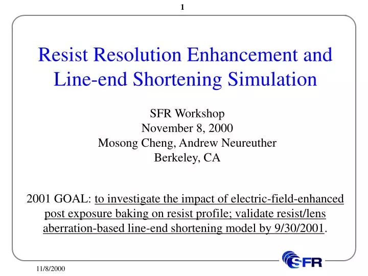
Resist Resolution Enhancement and Line-end Shortening Simulation. SFR Workshop November 8, 2000 Mosong Cheng, Andrew Neureuther Berkeley, CA.

E N D
Resist Resolution Enhancement and Line-end Shortening Simulation SFR Workshop November 8, 2000 Mosong Cheng, Andrew Neureuther Berkeley, CA 2001 GOAL: to investigate the impact of electric-field-enhanced post exposure baking on resist profile; validate resist/lens aberration-based line-end shortening model by 9/30/2001.
Electric-Field-Enhanced Post Exposure Bake • Vertical electric field enhance the vertical drift/oscillation of photoacid, improve resist profile uniformity, reduce lateral acid diffusion. • Al plates were coated a film to prevent electrochemical reaction • E: AC component and an upward DC component (to reduce T-topping).
Electric-Field-Enhanced vs. Standard Post Exposure Bake UVIIHS. 0.3, 0.2, 0.1mm L/S, 12mC/cm2. PEB 140oC, 90s. Dev. 60s. EFE-PEB: AC 9.8V, DC 0.65V, 3Hz. EFE-PEB E EFE-PEB E Standard
Electric-Field-Enhanced vs. Standard Post Exposure Bake EFE-PEB, 200nm CD Standard, 200nm CD EFE-PEB, 300nm CD UVIIHS. 0.3mm L/S, 9mC/cm2. PEB 140oC, 90s. Dev. 60s. EFE-PEB: AC 9.8V, DC 0.65V, 3Hz.
RIAR: Rapid Imaging Algorithm for Resist (SPIE Microlithography’00) • Assume 2-D reaction/diffusion. Parabolic polynomials are applied to approximate the solution. • Time evolving scheme: Iterative solve the polynomial coefficient until the error reaches certain criteria. CPU time of STORM=O(N2) CPU time of RIAR=O(N1.38) For 625 nodes, STORM 3min, RIAR 20sec.
Line-End Shortening: Calibrating Resist Model based on Pattern Fidelity Base model Tune chemically amplification coefficient Tune dissolution parameters Tune PEB diffusivity PROLITH simulation 2D image SEM image Differentiator
Calibrating Resist Model: Sim. Vs. Exp. II l=193nm,NA=0.6, s=0.75, resist thickness=350nm, Real mask CD data were used.
Applying the calibrated resist model to LES at the best focus SEM picture PROLITH simulation
2002 and 2003 Goals Investigate the impacts of the applied electric field polarity, frequency and magnitude on post exposure bake on e-beam and DUV exposure tools by 9/30/2002. Optimize the electric-field-enhanced post exposure baking process by 9/30/2003. Complete the resist/lens aberrations-based line-end shortening model and validate the simulation in 248nm and 193nm lithography by 9/30/2002.