Download
1 / 6
60 likes | 177 Views
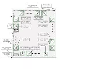
This document outlines the detailed specifications for chip design, including boundary coordinates, core locations, and pad positioning. The data includes precise measurements for various pads, as well as the coordinates for the chip's core and boundary. Key pads are identified with specific coordinate locations, with an emphasis on accuracy for integration into the overall chip design. The information is essential for engineers and designers working on device layout, ensuring proper placement during manufacturing.

E N D
68um 74um 3 3 3 3 3 3 3 3 3 3 3 3 68m CHDB(63) Chip Boundary Core 좌측하단좌표 ( 13, 13 ) Chip boundary 좌측하단좌표 ( 0, 0 ) Core 좌측하단좌표 ( 4377, 4377 ) Chip boundary 좌측하단좌표 ( 4350, 4350 ) 13um 110번 PAD 중심좌표 ( 3911, 4300) 144번 PAD 중심좌표 ( 312, 4300 ) 109번 PAD 중심좌표 ( 4038, 4300 ) 1번 PAD 중심좌표( 50, 4038 ) 74um 108번 PAD 중심좌표 ( 4300, 4038 ) 2번 PAD 중심좌표 ( 50, 3911 ) 74번 PAD 중심좌표 ( 4300, 439 ) 36번 PAD 중심좌표 ( 50 , 312 ) 73번 PAD 중심좌표 (4300, 312 ) 72번 PAD 중심좌표 ( 4038, 50 ) 37번 PAD 중심좌표 ( 312 , 50 ) 38번 PAD 중심좌표 ( 439 , 50 ) DEVICE LOGO
3 3 3 3 3 3 3 3 3 3 3 3 3 3 DEVICE LOGO Left Side PAD location
3 3 3 3 3 3 3 3 3 3 3 3 3 3 DEVICE LOGO Bottom Side PAD location
3 3 3 3 3 3 3 3 3 3 3 3 3 3 DEVICE LOGO Right Side PAD location
3 3 3 3 3 3 3 3 3 3 3 3 3 3 DEVICE LOGO Top Side PAD location