1 / 77

RHUMBA Concept

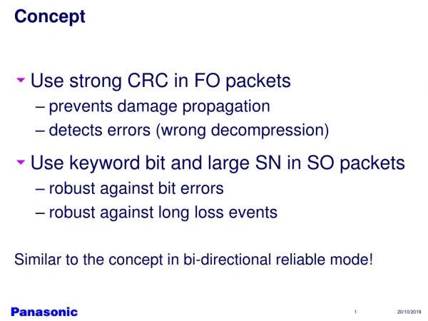
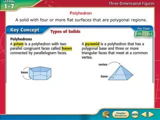
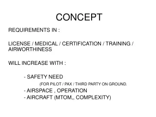
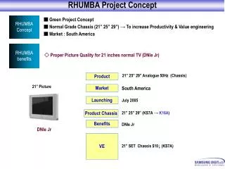
RHUMBA Project Concept. RHUMBA Concept. ■ Green Project Concept ■ Normal Grade Chassis (21” 25” 29”) → To increase Productivity & Value engineering ■ Market : South America. RHUMBA benefits. ◇ Proper Picture Quality for 21 inches normal TV (DNIe Jr). Product.

keelty
Download Presentation

RHUMBA Concept

An Image/Link below is provided (as is) to download presentation Download Policy: Content on the Website is provided to you AS IS for your information and personal use and may not be sold / licensed / shared on other websites without getting consent from its author. Content is provided to you AS IS for your information and personal use only. Download presentation by click this link. While downloading, if for some reason you are not able to download a presentation, the publisher may have deleted the file from their server. During download, if you can't get a presentation, the file might be deleted by the publisher.

E N D

Presentation Transcript


  1. RHUMBA Project Concept RHUMBA Concept ■ Green Project Concept ■ Normal Grade Chassis (21” 25” 29”) → To increase Productivity & Value engineering ■ Market : South America RHUMBA benefits ◇ Proper Picture Quality for 21 inches normal TV (DNIe Jr) Product 21” 25” 29” Analogue 50Hz (Chassis) 21” Picture South America Market July 2005 Launching 155W 105W Product Chassis 21” 25” 29” (KS7A → K16A) Benefits DNIe Jr DNIe Jr VE 21” SET Chassis $10↓ (KS7A)

  2. K16A Chassis Blocks Diagram

  3. Functional blocks UOCIII

  4. UOC3(TDA120XX) Pin Description

  5. Factory Data/Option1

  6. Factory Data/Option2

  7. Factory Data / Deflection

  8. Factory Data/Deflection

  9. Factory Data / Video Adjust 1

  10. Factory Data / Video Adjust 1

  11. Factory Data / Video Adjust2

  12. Factory Data/Video Adjust2

  13. Factory Data/Video Adjust2

  14. Factory Data/Video Adjust3

  15. Factory Data/Video Adjust4

  16. Factory Data/Video Adjust5

  17. Factory Data/Video Adjust5

  18. Factory Data/Video Adjust5

  19. Factory Data/YC Delay

  20. Factory Data/Others

  21. Factory Data/Others

  22. Factory Data/Others

  23. Pin configuration of “Face-down” QIP versions

  24. Control System Features ▶ 80C51 micro-controller core standard instruction set and timing ▶ 0.4883 ms machine cycle (6 clock cycles with 12.288 MHz derived from an xtal frequency of 24.576MHz) ▶maximum 256k x 8-bit program ROM ▶ maximum of 8k x 8-bit auxiliary RAM ▶ auxiliary RAM page pointer ▶ 12-level interrupt controller for individual enable/disable with two level priority ▶ stand-by, idle and power-down modes ▶ watchdog timer ▶ two 16-bit timer/counters ▶ additional 24-bit timer (16-bit timer with 8-bit Pre-scaler) ▶ 16-bit data pointer ▶ five 6-bit pulse width modulator (PWM) outputs for control of TV analogue signals. ▶ one 14-bit PWM for voltage synthesis tuning control. ▶ 8-bit ADC with 4 multiplexed inputs. ▶ remote control pre-processor (RCP). ▶ I2C byte level bus interface. ▶ universal asynchronous receiver transmitter (UART) ▶ 24 General I/O.

  25. 80C51 Microcontroller Block Diagram

  26. Flash Memory Block and Access Diagram

  27. TCG m-Controller Clock System Diagram

  28. Supply Scheme with Voltage Guards and Power On Reset Unit

  29. CVBS switch

  30. The UOCIII TV Sound Concept

  31. Overview of the UOCIII sound functions on the digital controller

  32. Overview of the UOCIII sound functions on the digital controller

  33. Overview of the UOCIII sound functions on the digital controller

  34. Overview of the UOCIII sound functions on the digital controller

  35. Demodulator and Decoder Block Diagram

  36. Signal processing modules

  37. Audio Backend Operation of UOCIII

  38. Syunc & Geometry block diagram

  39. IF block diagram

  40. Analogue sound block diagram

  41. Block diagram stereo sound processor

  42. CVBS I/O & Filters block diagram

  43. Chroma processing block diagram

  44. Chroma processing block diagram

  45. YUV processing block diagram

  46. RGB processing block diagram

  47. Cathode calibration loop block diagram

  48. UOCIII Pinning information

  49. UOCIII-N1D series Pinning information

  50. UOCIII-N1D series Pinning information

More Related