Download
1 / 60
650 likes | 1.12k Views
ANALOG - DIGITAL CONVERTERS Lecture 10. Analog to Digital Conversion. Introduction The sampling problem Conversion errors Different types of A-to-D converters Applications. Introduction to Analog to Digital Conversion. WHY TO GO TO DIGITAL WORDS ?

E N D
ANALOG - DIGITAL CONVERTERS Lecture 10
Analog to Digital Conversion • Introduction • The sampling problem • Conversion errors • Different types of A-to-D converters • Applications
Introduction to Analog to Digital Conversion • WHY TO GO TO DIGITAL WORDS ? • Benefits of Computer Power for further signal processing • Permanent Data Storage
Introduction to Analog to Digital Conversion • INTERFACE BETWEEN “ANALOGUE” SIGNALS AND DIGITAL (BINARY) REPRESENTATIONS • TWO ALTERATIONS OF THE SIGNAL: • Signal is sampled at given instants (sampling time) • Continuous amplitude is encoded to a limited number of binary word, i.e. a binary word represents an interval of amplitude (quantization) Binary code ….. Time 00101 00100 00011 00010 00001
Introduction to Analog to Digital Conversion • RESTITUTION OF THE SIGNAL THROUGH A DAC (Digital-to-Analogue Converter) • DIGITIZATION IS A CRUCIAL SIGNAL TRANSFORM and both transformations aspects (Time Sampling and Amplitude Quantization) have to be considered Binary code ….. 00101 00100 00011 00010 00001 Time
Max Quantization error : Q = +/- LSB/2 (ideal) Quantization noise : Introduction to Analog to Digital Conversion • Relationship between quantization error, number of bits, resolution: Binary code A = maximum amplitude Amplitude interval : LSB=A/2n n = number of bits ….. 00101 Ex : 8 bits ADC, 1V Full Scale Amplitude Resolution (LSB) = 1/28 = 3.9 mV (0.39%) 00100 00011 00010 00001
Introduction to Analog to Digital Conversion • Dynamic Range • Ratio between the minimum and the maximum amplitude to be measured • In case of a linear ADC, the dynamic range is related to the number of bits (and hence the resolution) • an 8-bit ADC has a dynamic range of 256 • In case of large dynamic range (as for calorimeter signals in HEP) the dynamic range could be as high as 2 106 : a linear ADC would require 21 bits! • Some non-linearity is then introduced and there is distinction between dynamic range and resolution • n-bit resolution • N-bit dynamic range (N>n) • example: • 12-bit resolution for a 16-bit dynamic range means that a signal in the range 1-65000 is measured with a resolution of 0.02%
Introduction to Analog to Digital Conversion • The perfect ADC would be the one with a very high number of quantization levels (high resolution) and at the same time very high sampling rate • Unfortunately this is not possible : different ADC architectures are existing, each one is offering a different compromise between resolution and sampling rate
Introduction to Analog to Digital Conversion Speed (sampling rate) • There is a trade-off between sampling rate and number of bits • The choice of an ADC architecture is driven by the application Power bipolar GHz >W Flash CMOS Sub-Ranging Pipeline Successive Approximation Sigma-Delta Discrete <mW Ramp Hz Number of bits 18 6
Sampling Frequency =2Hz The sampling problem 1 Hz signal • The sampling problem 2 Hz signal Sampling Frequency =1Hz • If sampling is done with rate of 1 Hertz (green points), blue and red curves can not be distinguished • To represent the 1 Hertz blue signal, at least two samples per period are needed (on picture, the additional purple point), i.e. sampling at 2 Hertz
The sampling problem • The sampling problem interpretations: • To represent a signal with maximum frequency f0, it is needed to sample at minimum frequency 2*f0 (Shannon Theorem) • Sampling at frequency fs is applicable to signals with bandwidth limited to fs/2 “analogue” signal spectrum • For conversion with an ADC sampling at frequency fs (Nyquist Rate ADC), the signal frequency bandwidth HAS TO BE LIMITED to fs/2
The sampling problem • Frequency representation of sampled signals “analogue” signal spectrum “sampled” signal spectrum “sampled” signal spectrum with first order “hold”
ADC errors : transfer curve • Ideal ADC • Errors • Offset • Integral non-linearity • Differential non-linearity • Missing code or non-monotonicity
Non Linearity ADC errors : Integral Non Linearity (INL) • Non linearity: maximum difference between the best linear fit and the ideal curve
ADC errors : Differential Non-Linearity (DNL) Code • Least Significant Bit (LSB) value should be constant but it is not • The difference with the ideal value shall not exceed 0.5 LSB • Easy way of seeing the effect • random input covering the full range • frequency histogram should be flat • differential non-linearity introduces structures -0.6LSB DNL +0.5LSB DNL Analog Input
ADC errors : Missing code, monotonicity • Other conversion errors : • non-monotonic ADC • Missing code Non-monotonic Missing code
q e(x) ADC errors : Effective number of bits (ENB) • An n bit ADC introduces a quantization error • Measurement of the SNR indicates the Effective number of bits ENB • Example: AD9235 12-bit 20 to 65 MHz • SNR (measured) = 70 dB • Effective number of bits = 11.4 • Encoding a signal (A/2) sinwt with A being the full scale will give an error • Ideal Signal to Noise Ratio
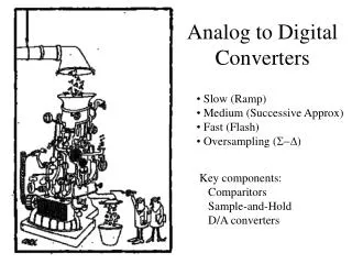
Types of ADC • Flash ADC & Subranging Flash ADC • Pipeline ADC • Successive Approximation ADC • Ramp ADC • Sigma-Delta
Flash ADC • Signal amplitude is compared to the set of 2n references • Direct “thermometric” measurement with 2n-1 comparators • Typical performance: • 4 to 10 bits (12 bits rare) • Up to GHz (extreme case) • High power (2n comparators) typ. 2W Sampling
Sub-ranging Flash ADC • Half-Flash ADC • 2-step Flash ADC technique • 1st flash conversion with 1/2 the precision • Residue calculation (1st flash conversion result reconstructed with a DAC and subtracted from signal) • Residue flash conversion • Typical performance: • 4 to 10 bits • Up to 100 MHz • Less power, but difficult analogue functions (sample and hold, subtraction, DAC) Required 4-bits + 4-bits sub-ranging flash needs 30 comparators (instead of 255 for 8-bits flash)
Pipeline ADC X 2 - S&H • Pipeline ADC • Input-to-output delay = n clocks for n stages • One output every clock cycle (as for Flash) • Saves power (N comparators) • Typ. 12 bits 40MHz 200mW Comparator 1-bit DAC 1-bit Sampling S&H Stage 1 Stage 2 Stage 3 Stage N Input ………… 1-bit 1-bit 1-bit 1-bit Time Adjustment & Digital Error Correction N-bit
Successive approximation • Compare the signal with an n-bit DAC output • Change the code until • DAC output = ADC input • An n-bit conversion requires n steps • Requires a Start and an End signals • Typical conversion time • 1 to 50 ms • Typical resolution • 8 to 12 bits • One comparator • Power • 10 mW S&H Input Sampling
Vin - + Counting time StartConversion StartConversion Enable S Q R N-bit Output Counter C Clk Oscillator IN Ramp ADC • Start to charge a capacitor at constant current • Count clock ticks during this time • Stop when the capacitor voltage reaches the input • Very slow, can reach very high resolution (1s, 18 bits) with some further tricks (dual slope conversion) (What’s used in digital multimeter) S&H Input
|e(f)| q f e(x) -fs/2 +fs/2 fs/2 fs/2 Over-sampling ADC • If fs/2 is higher than the maximum frequency f0 of the signal, then after filtering the quantization noise left in the signal frequency band (<f0) is : • Assuming the error is a white noise, its power spectral density is flat within the range [–fs/2,fs/2]
Over-sampling ADC (cont) • The signal to noise ratio when encoding a signal with maximum frequency f0 with sampling at fs • Hence it is possible to increase the resolution by increasing the sampling frequency and doing the proper filtering • Example : an 8-bit ADC would become a 12-bit ADC with an over-sampling factor of 250 (!) • But it is not an effective mean of increasing the resolution, because the 8-bit ADC must meet the linearity requirements of a 12-bit ADC
- Input Output 1-bit ADC 1-bit DAC 1rst Order Sigma-Delta Modulator Sigma-Delta ADC • Over-sampling ADC using a feedback loop to further reduce noise in the low-frequency range have been developed : the most common today is the Sigma-Delta Converter • The feedback loop provides a further “noise shape” with effective noise reduction in the signal frequency band
- Input Output 1-bit ADC 1-bit DAC 1rst Order Sigma-Delta Modulator Sigma-Delta ADC • This architecture is highly tolerant to components imperfections • With strong Noise shaping and high linearity capability, Sigma-Delta modulators are capable of very high resolution (up to 22 bits) • However some other limitations may appear and several complex architectures are derived from the “basic” schema
- Input Output 1-bit ADC 1-bit DAC 1rst Order Sigma-Delta Modulator Sigma-Delta ADC • The output of this modulator is a digital stream, whose average value is an approximation of the input signal. • Quantization error in case of a first-order • S-D converter: (Over-sampling ratio OSR=fs/2f0)
Sigma-Delta ADC (cont) • The signal to noise ratio when encoding a signal (A/2) sinwt, with A being the full scale, will be • Gain of 1.5 bits per each doubling of M • M = 2400 to have a 16-bit ADC • Higher orders sigma-delta are implemented to reduce OSR • Examples (Analog Devices) • 16-bit, 2.5 MHz • 24-bit, 1kHz
Applications • In HEP we are facing large number of channels • The quantity to be measured depends on the type of detector • Charge in the case of a lead glass calorimeter with PM read-out • Voltage in the case of a lead glass calorimeter with triode and preamplifier shaper read-out • We are facing fast signals (mean frequency ~ 12 MHz) • We are facing large dynamic range for calorimeter signals (up to 16 bits) • Flash ADC are commonly used, but it is a high power device, and there is no way to have one FADC per detector channel • Calorimeters signals are too fast for using S-D techniques
FADC for LHC trigger purpose (1) • Analog summation on the detector to form the trigger tower • Shaping time covers several bunch crossings • FADC and numerical filtering to: • Extract the energy • Extract the bunch crossing responsible for it
FADC for LHC trigger purpose (2) • Block diagram
ADC for an LHC calorimeter (1) • ATLAS Liquid Argon calorimeter • High dynamic range: 16-bit • Shaping of the signal to minimize pile-up • Sampling every 25 ns (bunch crossing period) • Level-1 pipeline Shaping
ADC for an LHC experiment (2) • Block diagram
ADC for an LHC experiment (3) • Performance • Pedestal stability to 0.1 ADC counts • Noise equivalent to 20 MeV • Integral non-linearity below 0.25% • Conversion time : 25 ns per sample
Digital Basics • Digital to Analog Converter • Takes a digital input and converts it to an analog voltage output. Digital Input: 0 – 255 Analog Output: 0 – 2.55V Resolution: ?? mV
Digital Basics • Digital to Analog Converter • Takes a digital input and converts it to an analog voltage output. Digital Input: 0 – 255 Analog Output: 0 – 2.55V Resolution: 10 mV
Digital Basics • Types of Digital to Analog Converters (DACs) • Current Summing DAC • R/2R Ladder DAC • Integrated Circuit DAC
Current Summing DAC All switches at GND IRF = IS2 + IS1 + IS0
Current Summing DAC All switches at GND IRF = IS2 + IS1 + IS0 IRF = 0 A + 0 A + 0 A = 0A
Current Summing DAC All switches at GND IRF = 0 A so VOUT = ?
Current Summing DAC All switches at GND IRF = 0 A so VOUT = 0 V
Current Summing DAC S2 at +2V, S1 & S0 at GND IRF = IS2 + IS1 + IS0
Current Summing DAC S2 at +2V, S1 & S0 at GND IRF = IS2 + IS1 + IS0 IRF = 2 mA + 0 A + 0 A = 2 mA
Current Summing DAC S2 at +2V, S1 & S0 at GND IRF = 2 mA so VOUT = ?
Current Summing DAC S2 at +2V, S1 & S0 at GND IRF = 2 mA so VOUT = -2.0V