Download
1 / 27
270 likes | 388 Views
Learn about small-signal analysis, load lines, Q-point, MOSFET parameters, and graphical analysis in FET amplifiers. Understand the characteristics and operations of common-source transistor amplifiers with practical circuit examples.

E N D
EMT 182ANALOGUE ELECTRONICS I Basic Field Effect Transistors Amplifiers
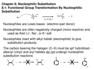
MOSFET AMPLIFIER Graphical Analysis, Load Lines Small-signal Parameters
Graphical Analysis, Load Lines Common-source transistor characteristic Load line equation? Q-point? IDQ VDSQ Shows DC load line, Q-point, VDS, as a result of sinusiodal source vi. A larger value of of vGS means a larger ID and smaller VDS. For negative vi, vGS decrease bias point moves down the load line. Time varying signal source vi, generates time varying components of gate-to-source, vGS, so, vGS = vi. For the FET to operate as a linear amplifier, transistor is biased in sat. region. iD and vDS must be in saturation.
If VGS leas than VTN, ID=0 (cut-off). • If VGS > VTN, transistor turns-on and biased in sat. region. • If VGS increases, Q-point moves up the load line. • Transition points-boundary between sat. and non-sat. region, defined as VDS = VDS (sat) = VGS – VTN. • As VGS increases above transition point, transistor biased in non-sat. region.
MOSFET Parameters • Instantaneous vGS: • DC or quiescent drain current, IDQ: • Time-varying drain current (linearly related to vGS): • Signal voltage proportional square: • Small signals implies linearity, means, total currents is total of dc and ac component of drain-current. • Then, small-signal ID related to small-signal vGS by Transconductance, gm • gm = id / vGS • Transconductance, gm is slope of VTN curve. If vgs small, gm is constant. gm0 is the gm value when VGS = 0
Small-signal: linearize the ac equivalent circuit. • Linear amplifier: the use of superposition so that the dc an ac analysis/signal of the circuits can be performed separately. Total response is the summation.
VDD vo id iD RD RD vO vgs + vi vDS + vGS - - vi VGSQ Small-signal Equivalent Circuit NMOS common source circuit with time-varying signal source in series with gate DC source AC equivalent circuit
vo id RD vgs vi Small-signal Equivalent Circuit • vO = vDS = VDD – iDRD • = VDD – (IDQ + id)RD • = (VDD – IDRD) - idRD • Small-signal parts: • vo = vds = -idRD • id = gmvgs • vi = vgs AC equivalent circuit
ids D + G + ids vgs gmvgs ro + vds vgs - - - S Small-signal Equivalent Circuit Common source NMOS with small signal parameters Simplified small signal equivalent circuit for NMOS Small-signal output resistance where λ, Channel-length modulation parameter.
VDD VDD ID RD RD R1 R1 iD vO 0 + CC vG VG VDS - + VGS R2 - vi R2 DC Analysis – Saturation Region Voltage-divider circuit for MOSFET DC equivalent circuit
VDD ID RD R1 0 + VG VDS - + VGS R2 - DC Analysis– Saturation Region DC equivalent circuit
VDD 5 V 20 k 30 k RD R1 iD vO CC vG vi R2 20 k Example VTN = 1 V K = 0.1 mA/V2
VDD RD R1 ID + 0 VG VDS + - VGS R2 - DC equivalent circuit The transistor is biased in the saturation region because VDS > VDS(sat) = VGS – VTN = 2 – 1 = 1 V
MOSFET AMPLIFIER Common-Source Amplifier Equivalent circuit With source resistor With source bypass capacitor Common-Drain Amplifier Common-Gate Amplifier
COMMON-SOURCE AMPLIFIER- Basic Configuration Common-source circuit with voltage divider biasing & coupling capacitor • Signal is coupled into gate through coupling capacitor, Cc. • Cc will provide dc isolation between amplifier and signal source. • DC biasing established by R1, R2.
Small-signal equivalent circuit input resistance output voltage Vo = - gm Vgs (ro || RD) input voltage Ro = RD || ro output resistance ro = VA / IDQ small-signal voltage gain - We assume that capacitor essentially a short circuit to signals.
iD Transition point Q-point IDQ vDS VDSQ VDD DC Load Line RK 86 DC load line & transition point • Transition point: separate sat. and non-sat. region. • Q-point must be near mid of sat. region to provide max symmetrical output voltage and keep the transistor biased in sat. region.
+VDD 12V RD 3 k C2 R1 vo 300 k C1 RSi RL 2 k 3 k R2 200 k vi RS 2 k COMMON-SOURCE AMPLIFIER - with Source Resistor CALCULATION EXAMPLE Given: VTN = 2V, K = 1 mA/V2, = 0 Determine: i- Q-point values (ID , VDS) ii- small-signal voltage gain • Stabilize the Q-point against variation of transistor parameters. • When kn varies, the Q-point will not vary much if Rs included.
VDD=12V RD=3 k R1=300 k VG R2=200 k RS=2 k Q-point values dc equivalent circuit
Q-point values (Cont) So, the Q point value:
RSi Vo + Vi R1||R2 RD||RL Vgs gmVgs _ RS Small-signal analysis
+VDD RD C2 R1 C1 RSi RL vo R2 vi C3 RS COMMON-SOURCE AMPLIFIER - with Bypass Capacitor • Required to provide small impedance at all frequencies • Lower signal frequency, less effective bypass capacitor. Minimize the lost in small-signal voltage gain while maintaining the Q-point stability
RSi Vo + Vi R1||R2 Vgs ro RD||RL gmVgs _ Ri Small signal equivalent circuit
+VDD R1 C1 RSi C2 vi R2 RS RL vo RK 05 COMMON-DRAIN AMPLIFIER • Output signal, vo taken off the source. • Drain connected directly to VDD. • VDD become signal ground in ac equivalent circuit.
Small signal equivalent circuit RSi Vin _ + Vo Vgs ro Vi gmVgs R1||R2 RS||RL input impedance Output impedance input voltage output voltage small-signal voltage gain • Assume Cc acts as a short circuit. • Drain at signal ground. • Small signal resistance, ro parallel with current source.
COMMON-GATE AMPLIFIER V+ RD RSi C1 C2 vi IQ RL vo RG C3 V - • Input signal is applied to the source terminal. • Gate is at signal ground. • RG prevents the build up of static charge on gate terminal. • CG ensure the gate at signal ground. • CC1 couples signal to source. • CC2 couples output voltage to RL.
Ri gmVgs RSi Vo _ Ii Vgs Vi RD RL + Small-signal equivalent circuit • ro assume infinite. • Source at the input. input impedance output voltage input voltage small-signal voltage gain input current