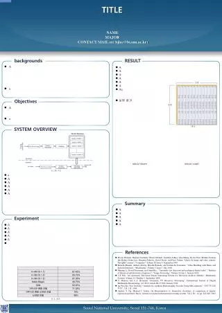
*The Result*
*The Result*. C ontents : 9( v ) 5( v ) 레귤레이터 IC NE555 타이머 발진회로 10 진 카운터 6 진 카운터 채터링 현상 회로도와 브레드보드 결선도. <2 조 Digital Stop Watch 최종 구성 블록도 > . 1. 9[V]→5[V] 레귤레이터 ① 9[v]→5[v] 레귤레이터 회로


*The Result*
E N D
Presentation Transcript
Contents : 9(v) 5(v) 레귤레이터 IC NE555 타이머 발진회로 10진 카운터 6진 카운터 채터링 현상 회로도와브레드보드 결선도
1.9[V]→5[V] 레귤레이터 ① 9[v]→5[v] 레귤레이터 회로 이번 설계에서 사용되는 모든 IC의 정격전압이 4.5~5.5[V]이기 때문에 DC 건전지 9[V]의 전압을 레귤레이터를 이용하여 5[V]로 강하시켜준다. <그림01-IC7805를 이용한 9[V]→5[V] 레귤레이터 회로도>
② Pspice시뮬레이션 결과 < 그림02-Pspice를 이용한 시뮬레이션> ※ 시뮬레이션 결과 DC 9[V]의 전압이 4.997[V]로 대략 5[V]로 변환되는 것을 볼 수 있다.
2. IC NE555 타이머 발진회로 ① 비안정멀티바이브레이터의구동원리 The capacitor C charges via R1 and R2 and when the voltage on the capacitor reaches 2/3 of the supply, pin 6 detects this and pin 7 connects to 0v. The capacitor discharges through R2 until its voltage is 1/3 of the supply and pin 2 detectsthis and turns off pin 7 to repeat the cycle. The top resistor iprevent pin 7 being damaged as it shorts to 0v when pin 6 detects 2/3 rail voltage. s included to Its resistance is small compared to R2 and does not come into the timing of the oscillator. <그림03-비안정멀티바이브레이터발진회로>
② 비안정멀티바이브레이터의주파수 그래프 Using the graph: Suppose R1 = 1k, R2 = 10k and C = 0.1u(100n). Using the formula on the graph, the total resistance = 1 + 10 + 10 = 21k The scales on the graph are logarithmic so that 21k is approximately near the "1" on the 10k. Draw a line parallel to the lines on the graph and where it crosses the 0.1u line, is the answer. The result is approx 900Hz. <그림04-적용된 주파수 그래프>
③비안정멀티바이브레이터의공식 및 주파수조건표 Using the picture, The frequency of an astable circuit can also be worked out from the following formula:
④ 100[Hz]를 발진하는 비안정멀티바이브레이터 <그림05-IC NE555타이머를 이용한 100[Hz]발진회로>
⑤ Pspice시뮬레이션 결과 <그림06-Pspice를 이용한 시뮬레이션> ※ 시뮬레이션 결과0.1[s](100[ms])동안 대략 10주기를 갖는 것을 볼 수 있으며 1[s]동안 대략 100주기를 갖는 다는 것을 예상할 수 있다.
3. 10진 카운터 -제안서에서 계획했던 IC 7490 10진 카운터 대신에 BCD UP/DOWN Counter인 IC HD74LS192를 사용하기로 결정하였다. <그림07-IC> * HD74LS192의 핀배치도 및 특징* <그림08-IC> *HD74LS192의 Counter Sequence*
*IC HD74LS192의 MOD-10 동작 및 시뮬레이션(10진 카운터) <그림09-7447 디코더 드라이버에 연결한 MOD-10 회로> *<그림10 > Pspice를 이용한 시뮬레이션 ※ 시뮬레이션 결과 0~9까지 카운트 되는 것을 확인 할 수 있다.
4. 6진 카운터 ① IC HD74LS192의 MOD-6 동작 (6진 카운터) <그림11-7447 디코더 드라이버에 연결한 MOD-6 회로> ※ Q2,Q3의 출력을 AND게이트를 이용하여 IC HD74LS192의 RESET 보조입력단자에 인가하여 MOD-6으로 동작하도록 하였다.
② Pspice시뮬레이션 결과 <그림12-Pspice를 이용한 시뮬레이션> ※시뮬레이션 결과 0~5까지 카운트 되는 것을 확인 할 수 있다.
5. 채터링 현상과 슈미트트리거에 의한 채터링 방지 <그림01 > - 채터링현상을 보기 위한 일반 스위칭 회로> <그림02 > - 슈미트트리거에 의한 채터링 방지 회로>
② *STOP Switch의 채터링 관찰 <그림02- STOP switch 회로> *오실로스코프로 관측한 채터링 현상 ※ '0'→'1'로 스위칭 될 경우 채터링 현상이 발생함을 관측할 수 있었다. '1'→'0' 스위칭 될 경우 '0'→'1'로 스위칭 시 보다 지연시간이 긴 것을 관측할 수 있었다.
3. 시뮬레이션 결과 - 스위칭 될 경우 직접적인 채터링 현상을 확인 할 수 없으나 슈미트트리거에 의한 결과를 통하여 채터링현상이 사라진 것을 확인 할 수 있다. <그림03- Pspice시뮬레이션 결과> ※노란선: 스위칭 결과 / 초록선: 슈미트트리거에 의한 출력 결과
*STOP switch의 채터링 관찰 <그림07- 슈미트트리거에 의한 채터링 방지 회로>
*STOP switch의 채터링오실로스코프로 관측한 파형 <그림09- '1'→'0'의 파형> <그림08- '0'→'1'의 파형> ※'0'→'1'로 스위칭할 경우 발생하던 채터링 현상이 사라진 것을 관측할 수 있었다. '1'→'0' 스위칭할 경우 '0'→'1'로 스위칭 시 보다 지연시간이 길었는데 관측결과 지연시간이 사라진 것을 관측할 수 있었다.
*브레드보드에 연결한 전체회로도 ➂7-segment display ➃Counter및 RAB time load ➀5[V] Regulator ➁555 Timer - 100[Hz] ➄Stop Switch / reset, RAB save push button
*➀5[V] Regulator <결선도> <브레드보드 회로도>
* ➁555 Timer - 100[Hz] <555Timer – 100(Hz)발진 브레드보드> <결선도>
*➂7-segment display <결선도> <브레드보드 회로도>
* ➃Counter및 RAB time load <브레드보드 회로도> <결선도>
* ➄Stop Switch / reset, RAB save push buttonn ※ 7400과 7486을 이용한 스위치 감축 - 일반 손목전자시계의 설정과 비슷하게 구현
*RAB time 출력Switch <브레드보드 회로도> <결선도>
* 문제 해결* troubleshooting -*74192의 6진 Counter 로의 변환에서 발생하는 문제 해결*
Summary: 실제 스탑워치와 유사하게 하기 위해 최소화 하려 노력. 스위치 수의 최소화 (시중의 StopWatch와 유사하여 조작이 용이) 3. IC소자의 통일성과 갯수의 최소화(기타 오류 발생 가능성이 낮아짐) 4. HD74LS192 를 통한 동기식 카운터의 구현 5. 7segment 6EA로 RAP TIME 을 확인