Download
1 / 1
10 likes | 100 Views
Explore quantum effects on ultrathin Pb films on silicon using x-ray diffraction, observing unique growth behaviors and structure fluctuations. Dive deep into quantum oscillations, layer-by-layer growth modes, and Friedel-like charge density variations. Discover the impact of electronic properties on film morphology, layer relaxations, and magic island formation, with implications for nanostructure development.

E N D
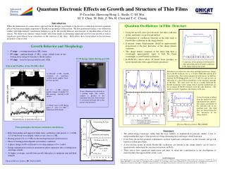
CCD Image taken during growth Pb(10L) Si(10L) Reflectivity X-rays illuminate the substrate at a grazing angle. The surface normal is parallel to the horizontal direction. Direct beam is at bottom left-hand side of the picture (not pictured). oscillations and beating magic islands wetting layer Quantum Electronic Effects on Growth and Structure of Thin Films P. Czoschke, Hawoong Hong, L. Basile, C.-M. Wei, M. Y. Chou, M. Holt, Z. Wu, H. Chen and T.-C. Chiang Introduction When the dimensions of a nano-device approach the de Broglie wavelength of the device’s conduction electrons, quantum effects become increasingly important to the physical properties of the system. We have performed surface x-ray diffraction studies with high-intensity synchrotron radiation to probe the growth behavior and structure of ultrathin films of lead on silicon. We observe an unusual “magic height” effect that results in alternating island and layer-by-layer growth as well as significant quasi-bilayer layer relaxations in the structure of the films. Both effects have been linked to the electronic properties of the system. Quantum Oscillations in Film Structure • Using the layer-by-layer growth mode, flat films with near atomic uniformity are grown and studied. • Confinement of conduction electrons in the film leads to Friedel-like oscillations in the charge density. • If present, atomic displacements should be approximately proportional to the first derivative of the charge density variations. • The charge density variations in the metal film have a wavelength approximately equal to half the Fermi wavelength, as with Friedel oscillations. • In Pb/Si(111), this is about 1.8 atomic layer spacings, so layers should relax with a quasi-bilayer periodicity. Growth Behavior and Morphology • 1st stage - a wetting monolayer (ML) forms • 2nd stage - uniform-height (5 ML) magic islands form on the wetting layer and grow laterally to fill the surface • 3rd stage - layer-by-layer growth beyond 6 ML A schematic of the quantum well formed by a thin metal film and the Friedel oscillations in the charge density that result. Extracted Profiles of the Pb(10L) Rod Extended x-ray reflectivity data show multiple interference fringes due to the Pb overlayers for (a) a 10 layer thick film and (b) an 8 layer thick film. The features pointed out with arrows are halfway between the Pb Bragg peaks (at l = 3.3 and 6.6) and are thus an indication of a quasi-bilayer periodicity in the interlayer spacings of the film. The solid curves are fits to a model following the Friedel oscillations of the charge density and the dashed lines are fits assuming all the Pb overlayers have the same thickness. The model accurately reproduces the features of the data. (a) Beyond ~6 ML, smooth evolution of multilayer satellite peaks implies layer-by-layer growth (b) 1.5 – 6 ML, constant profile; islands of height 51 ML growing laterally to fill surface Layer relaxations resulting from the model fits to the experimental data (points). The origin corresponds to the substrate side of the quantum well. The solid lines are derived from the first derivative of the charge density. (c) Sharp onset of Pb Bragg peaks at ~350s (1.5 ML) – formation of Pb islands Physical Review Letters, 91, 226801 First-principles electronic structure calculations • Summary • The global energy landscape, rather then the local stability as emphasized in previous studies, is key to understanding this type of film growth involving alternating layer and magic-island formation. • It has been shown that quantum confinement can have significant consequences on the structure and growth behavior of thin metal films. • A free-electron model in which Friedel-like oscillations are present in the charge density can be used to quantitatively understand the structural relaxations in Pb/Si. • These effects have significant implications and must be taken into consideration in the development of nanostructures that approach the atomic scale. • Both freestanding and supported films show oscillations with period = 1.8 ML (1/2 of the Fermi wave length), which is very close to 2 ML. • Beating period /(2-)= 9 ML for the envelope function (dotted curves) • Phase of beating pattern depends on boundary conditions • A phase change for Pb on Si leads to two deep minima at N = 1 and 6. • Energy minimization results in spontaneous phase separation into a wetting layer and magic islands. • At higher coverages, smooth layer growth takes place to minimize step and kink energies • Physical Review Letters, 90,76104 (2003) Acknowledgements The UNICAT facility at the Advanced Photon Source (APS) is supported by the University of Illinois at Urbana-Champaign, Materials Research Laboratory (U.S. DOE, the State of Illinois-IBHE-HECA, and the NSF), the Oak Ridge National Laboratory (U.S. DOE under contract with UT-Battelle LLC), the National Institute of Standards and Technology (U.S. Department of Commerce) and UOP LLC. The APS is supported by the U.S. DOE, Basic Energy Sciences, Office of Science under contract No. W-31-109-ENG-38.