Download
1 / 20
200 likes | 331 Views
This investigation explores innovative network-based interconnect systems tailored for current and future FPGA architectures. As semiconductor technology evolves, traditional methods of chip interconnection become limiting factors impacting performance. This research introduces a scalable network-on-chip solution to address the challenges posed by rising chip complexity and wiring congestion. Two types of network systems—packet and circuit switching—will be designed, implemented, and tested to evaluate their performance and hardware costs, ultimately offering insights for next-generation FPGA designs.

E N D
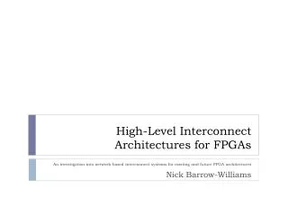
High-Level Interconnect Architectures for FPGAs An investigation into network-based interconnect systems for existing and future FPGA architectures Nick Barrow-Williams
Introduction • Semiconductor industry has grown rapidly for several decades • Continued shrinking of device dimension introduces new design challenges • Moving data around a chip can now be the limiting factor of performance • Existing solutions do not scale well
Why do existing solutions not scale? • Die size has been growing consistently • Global connections are longer • Wire depth increased to counter width decrease • Parasitic capacitive effects increase and cause slow signal propagation
Why do existing solutions not scale? • Existing system-level connection uses buses • Buses increase resource efficiency and decrease wiring congestion • Not suitable for a large number of modules • A network based alternative would offer higher aggregate bandwidth
Why design for FPGA systems? • FPGA market growth sustained for several years • FPGA silicon area already dominated by wiring • Global wires are limited in number • Increasing gate count only increases wiring congestion
The Solution: Network-on-Chip • Use technologies from network systems • Replace inefficient global wiring with high-level interconnection network • Create scalable systems to handle large numbers of modules • Use high metal layers to avoid parasitic effects
Existing Solutions • Most existing systems are for ASIC designs • Stanford Interconnect • RAW • SCALE • SPIN • PNoC: An solution for FPGAs • Complex • High hardware cost • Other simulated solutions exist but few are implemented
Proposal: Two network systems • Existing solutions use either packet switching or circuit switching techniques • Design, implement, test and synthesise one of each to compare performance and hardware cost • Map solutions to an FPGA platform to evaluate hardware cost in current generation systems
Network Architecture Design • Topology • Simple • Scalable • Low wiring requirements • Solution: 2D mesh Topology
Network Architecture Design • Routing Algorithm • Deterministic • Data always follows same path through network • Simple hardware • Sensitive to congestion • Adaptive • Paths through network can change according to load • Complex hardware • Avoids congestion
Network Architecture Design • When choosing routing algorithms must avoid: • Deadlock: • Livelock Solution: Use unidirectional wiring and allow each node to make two connection Solution: Use deterministic routing
Network Architecture Design • Flow control methods • Circuit switched • Circuit request propagates through network • Path reserved to destination • Grant signal propagates back • Data sent then circuit deallocated • Packet switched • Use header, body and tail • Wormhole routing • Forward header and body without waiting for tail • Need buffers to store stalled packets
Router Design • Each router contains a number of modules • FIFOs (only present in packet switched router) • Address to port-request decoder • Arbiter • Control finite state machines • Crossbar
Addresses In Router Address Logic Logic Logic Logic Logic Registers Port Requests Out Router Design: Address decoder • Takes addresses from each five input ports • Outputs the direction to route the packet
In Port Out Port Requests Out Requests In FSM Grant In Grant Out Router Design: Control FSMs • Each FSM has multiplexed inputs and outputs • Reduces the size of the FSM considerably • Example here is from circuit switched router
Router Design: Crossbar • Each crossbar can make two connections to avoid deadlock • Pipelined design to increase router throughput In Port x 2 Out Port x 2 Data Out Data In
Circuit Switched Router Structure Data In Arbiter Address to Port Decoder Request In In & Out Ports FSM Request Out Request In Grant Out Grant In Data In Crossbar Data Out
Packet Switched Router Structure Data From FIFOs Arbiter Address to Port Decoder Write Request From FIFOs Write FIFO FSM Req FIFO FSM Req Data In Grant Data In Grant Full Full Data In & Out Ports Control Write Out 5 x Queue Request In Grant Out Full In Data From FIFOs Crossbar Data Out Data
Router Implementation and Testing • Both routers were coded using VHDL • Simulation and testing used a combination of ModelSim and Xilinx ISE 9.1 • Ad-hoc tests used for individual modules • VHDL testbench used for system verification
Testbench Structure TESTBENCH Clock Gen Reset Gen Cycle Count Mesh Network Input Tables #START SOURCE DEST SIZE ID # ------------------------------------------------------ 2 3 0 0 1 8 1 3 2 0 0 1 2 2 3 2 3 1 1 2 3 4 3 1 1 0 8 4 5 0 3 1 3 7 5 Source Sink Command File Output Table Test Table Read Input Compare Output File Success: ID: 1 Source : (0,3) Dest : (1,0) Hops : 4 Latency: 34 Success: ID: 2 Source : (0,2) Dest : (1,0) Hops : 3 Latency: 27 Success: ID: 3 Source : (3,2) Dest : (1,1) Hops : 3 Latency: 22 Success: ID: 4 Source : (1,3) Dest : (0,1) Hops : 3 Latency: 22 Success: ID: 5 Source : (3,0) Dest : (3,1) Hops : 1 Latency: 12