Clocks
250 likes | 269 Views
Learn about clock signals, state elements, set-reset latches, gated D-latches, and more crucial concepts in digital logic design.

Clocks
E N D
Presentation Transcript
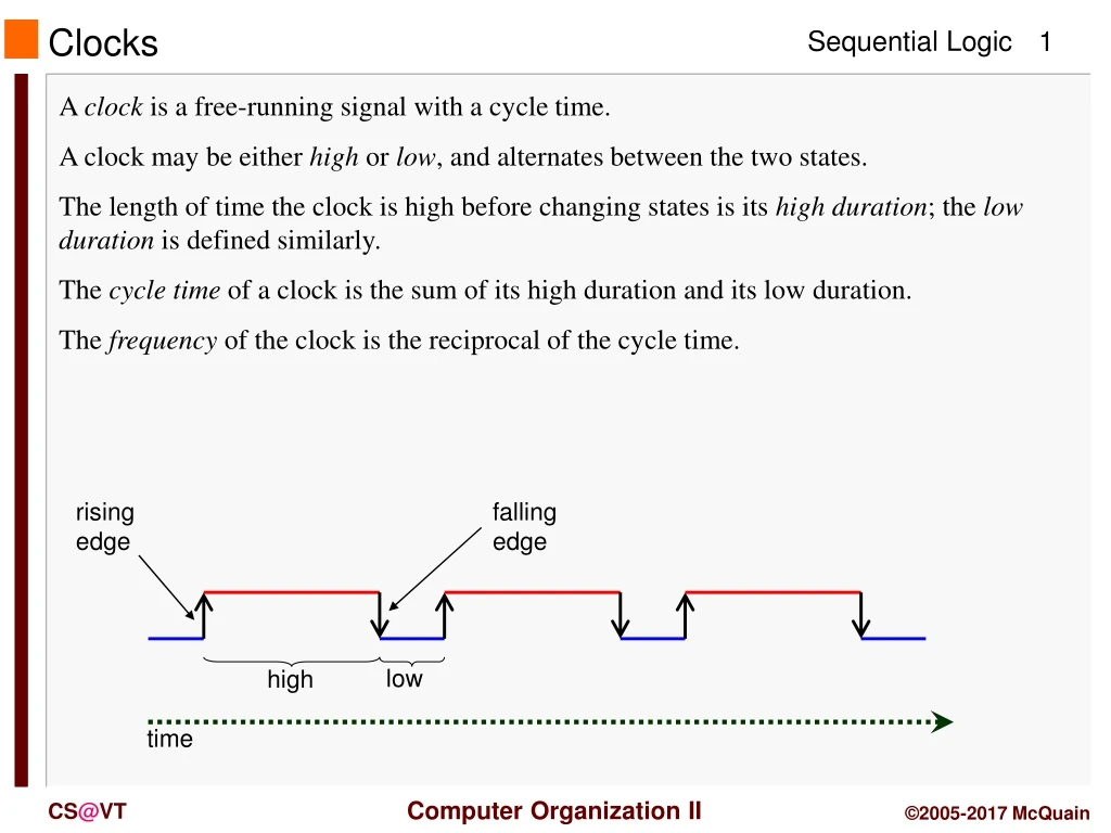
rising edge falling edge low high time Clocks A clock is a free-running signal with a cycle time. A clock may be either high or low, and alternates between the two states. The length of time the clock is high before changing states is its high duration; the low duration is defined similarly. The cycle time of a clock is the sum of its high duration and its low duration. The frequency of the clock is the reciprocal of the cycle time.
State Elements A state element is a circuit component that is capable of storing a value. • A state element may be either unclocked or clocked. • Clocked state elements are used in synchronous logic • - When should an element that contains state be updated? • - Edge-triggered clocking means that the state changes either on the rising or the falling edge. • - Clock edge acts as a sampling signal that triggers the update of a state element. • A signal that is to be written into a state element must be stable; i.e., it must be unchanging. • If a function is to be computed in one clock cycle, then the clock period must be long enough to allow all the relevant signals to become stable.
Set-reset Latch A latch is a circuit that has two stable states, and so can store 1 bit of data. NOR gate output is only 1 when both inputs are 0 If the output of one NOR gate is 1 then the output of the other must be 0 Feedback: output depends both on present inputs and past inputs Common contemporary terminology is that a latch does not receive a clock signal, and hence is transparent. However, usage does vary…
Set-reset Latch Details Here's an initial state: First, let's understand why this is a stable state. Consider the upper NOR gate: it's receiving two 0's, and hence will output a 1. Therefore, the lower NOR gate will receive one 0 and one 1, and hence it will output a 0. 0 0 1 0 And... the current state is stable... Now, consider what happens if we toggle one of the inputs…
Set-reset Latch Details 1: Suppose we toggle R to 1 2: Then the upper NOR gate receives a 1 and a 0 and emits 0 1 0 1 4: Then, the upper NOR gate receives two 1's and continues to emit 0… stability! 0 1 3: Then, the lower NOR gate receives two 0's and emits 1 So, turning R(eset) on toggles the SR latch (from storing 1) to store 0. And… turning R(eset) off now doesn't change the state of the latch.
Set-reset Latch Details 3: Then, the upper NOR gate receives two 0's and emits 1 1 1 0 1 0 1: Suppose we toggle S to 1 1 2: Then the lower NOR gate receives a 1 and a 0 and emits 0 4: Then, the lower NOR gate receives two 1's and continues to emit 0… stability! So, turning S(et) on toggles the SR latch (from storing 0) to store 1. And… turning S(et) off now doesn't change the state of the latch.
Gated D-latch • The gated D-latch can be derived from the set-reset latch by adding an interface that makes it possible to essentially isolate the set-reset logic: If the Enable input is 1 then the value of D will immediately be stored by the S-R mechanism. If the Enable input is 0 then the value of the S-R mechanism is fixed. The S = R = 1 case cannot occur for the embedded S-R latch, because…
Timing Issues • There is a small, but positive delay between changes in the input values to a logic gate and any resulting change in the gate's output. We call this the gate delay. • Consider the following circuit: Logically, the output of the circuit should ALWAYS be 0. Why? Consider what happens if the input signal A is set to 1: - A0, A1 and A2 immediately become 1 - after one gate delay, the output X will become 1 since the XOR has inputs of 0 and 1 - at the same time, the output of the AND gate will become 1 - after one more gate delay, the output X will become 0 again What would happen if the output X were used as input to another circuit? We can prevent that if we use a clock signal to synchronize operations.
Clocked D-latch • We create a clocked D-latch by connecting the Enable input of the gated D-latch to a clock signal: The clocked D-latch accepts the input D only when the clock signal is high (1). However, there is still a hazard… what if the value of D can change more than once during the high-duration of the clock signal? The clocked D-latch is level-triggered… that is, whether its state can change depends on the level of the clock signal.
clocked S-R latch 2 gate delays Clocked D Flip-flop • Consider what happens when we combine a clocked D-latch and a clocked S-R latch: clocked D-latch D inverted clock Assuming the Enable input is 1, the output of the device can only change once per clock cycle… shortly after the clock signal goes low. If Enable is 0, then the circuit always sees the clock signal as 0, and nothing changes.
clocked S-R latch Clocked D Flip-flop • Suppose that D is set to 1; nothing happens at all until the clock signal also goes high: clocked D-latch The output of the D-latch goes high (i.e., takes the value of D) but only after two gate delays. By then, the S-R latch is seeing a low clock signal, and so the S-R latch does not change state yet.
clocked S-R latch Clocked D Flip-flop • Then, when the clock goes low… clocked D-latch D The S-R latch sees a high clock signal (after 1 gate delay), and so it updates state. But, the D-latch sees a low clock signal immediately and so it cannot change state.
clocked S-R latch Clocked D Flip-flop • Then, when the clock goes low… clocked D-latch D And, when Enable is turned off, the flip-flop is in a locked state.
4-Bit Register • Built using D flip-flops: Clock input controls when input is "written" to the individual D flip-flops. This is easily scaled to store a wider data value.
Design: a mod-8 Counter A mod-8 counter stores a integer value, and increments that value (say) on each clock tick, and wraps around to 0 if the previous stored value was 7. So, the stored value follows a cycle: 000 001 010 011 100 101 110 111 000 . . .
Design: State Machine We need eight different states for our counter, one for each value from 0 to 7. We can describe the operation by drawing a state machine. The nodes represent states and the edges represent transitions and are labeled with the input (clock in this case) that causes the transition to occur. 0 0 0 0 1 1 1 101 011 010 001 000 111 110 100 1 1 1 1 1 0 0 0 0
Design: State Table A state table summarizes the state machine and is useful in deriving equations later: Current State Input Next State ------------------------------------ 0 0 0 1 0 0 1 0 0 1 1 0 1 0 0 1 0 1 0 1 1 0 1 1 1 1 0 0 1 0 0 1 1 0 1 1 0 1 1 1 1 0 1 1 0 1 1 1 1 1 1 1 1 0 0 0 1 1 1 100 000 101 110 111 011 010 001 1 1 1 1 1
Design: Deriving Equations We will derive an equation for each of the next state functions: Current State Input Next State C2 C1 C0 N2 N1 N0 ------------------------------------ 0 0 0 1 0 0 1 0 0 1 1 0 1 0 0 1 0 1 0 1 1 0 1 1 1 1 0 0 1 0 0 1 1 0 1 1 0 1 1 1 1 0 1 1 0 1 1 1 1 1 1 1 1 0 0 0
Design: Mapping to D Flip-flops Since each state is represented by a 3-bit integer, we can represent the states by using a collection of three flip-flops (more-or-less a mini-register). We will implement the circuit using D flip-flops, which make for a simple translation from the state table because a D flip-flop simply accepts its input value. D Q ~Q ------------ 0 0 0 0 1 0 1 0 1 1 1 1 So, we just need to feed each of the flip-flops the value of the appropriate next-state function equation derived earlier…
D Q CK ~Q D Flip-flop The D flip-flop takes one data input and updates its state Q, on a clock tick, according to its excitation table: D Q ~Q ------------ 0 0 1 1 1 0 In the following Logisim diagrams, the D flip-flops update state on the falling edge (when the clock goes from high to low).
J Q CK K ~Q JK Flip-flop The JK flip-flop takes two data inputs and updates its state Q, on a clock tick, according to the table: J K Q ~Q ---------------------- 0 0 no change 0 1 0 1 1 0 1 0 1 1 opposite In the following Logisim diagrams, the JK flip-flops update state on the falling edge (when the clock goes from high to low).
A mod-16 Counter We can use JK flip-flops to implement a 4-bit counter: Note that the J and K inputs are all set to the fixed value 1, so the flip-flops "toggle". As the clock signal runs, the circuit will cycle its outputs through the values 0000, 0001, 0010, . . . , 1111, 0000, . . . and then repeat the pattern. So, it counts clock ticks, modulo 16.
mod-16 Counter: first tick Suppose the counter is in the initial state shown below (output is 0000). When the clock cycles from high to low: - the right-most sees its (inverted) clock signal go from low to high, and so it toggles its state to 1 - the next flip-flop sees its clock signal go from high to low, and so it doesn't toggle - and so, neither do the other flip-flops… So, the output is 0001: