
Chapter14
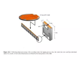
Figure 14.1: Following planar processing of the recording wafer, the lapping process dices the wafer into rows and then individual sliders As a result, several critical dimensions are defined by the final position of the ABS.

Chapter14
E N D
Presentation Transcript
Figure 14.1: Following planar processing of the recording wafer, the lapping process dices the wafer into rows and then individual sliders As a result, several critical dimensions are defined by the final position of the ABS.
Figure 14.2: Schematic illustration of the magnetic recording process. A thin film head flies above the medium at a height d. A write element of width Pw orients the magnetization in the media. A read element of width MRw detects the fringing field from the magnetic transitions in the media.
Figure 14.3: a) SEM image of a 40 Gbit/in2 recording head viewed from the ABS. The sensor is located beneath the writer. The writer width, Pw, is 350 nm. The write gap, g, is 100 nm. b) Perspective view schematic of the recording head illustrating how flux is carried from the coils to the ABS.
Figure 14.4: a) TEM image of a 40 Gbit/in2 sensor viewed from the ABS. b) Schematic diagram of the sensor.
Figure 14.5: a) Historical trends in integrated circuit features and thin film head features (projection from 2000 based on 60% areal density growth and 50% decrease in integrated circuit features every 6 years).
Figure 14.5: b) Scaling trends for this decade. The areal density corresponding to the feature size is shown above the graph.
Figure 14.6 SEM image of plated pole tip feature. The resist stencil defined with 100 keV e-beam lithography was 2 mm tall and 200 nm wide. A line is drawn to Show where lapping would define the ABS.
Figure 14.7: a) TEM image of a CPP sensor viewed from the ABS. b) Schematic diagram of the sensor. The hard bias is insulated from the sensor by a thin layer of alumina. The tunnel barrier in the sensor is the thin white line visible in the TEM micrograph.