Download
1 / 2
20 likes | 142 Views
Understanding the Growth and Performance of Antimonide Nanowire Chen Yang, Purdue University, DMR 0847523.

E N D
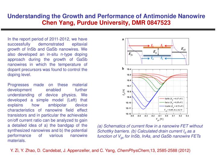
Understanding the Growth and Performance of Antimonide NanowireChen Yang, Purdue University, DMR 0847523 In the report period of 2011-2012, we have successfully demonstrated epitaxial growth of InSb and GaSb nanowires. We also developed an in-situ n-type doping approach during the growth of GaSb nanowires in which the temperature of dopant precursors was found to control the doping level. Progresses made on these material development enabled further understanding of device physics. We developed a simple model (Left) that explains how ambipolar device characteristics of nanowire field effect transistors and in particular the achievable on/off current ratio can be analyzed to gain a detailed idea of a) the bandgap of the synthesized nanowires and b) the potential performance of various nanowire materials. (a) Schematics of current flow in a nanowire FET without Schottky barriers. (b) Calculated drain current Id as a function of Vgs for InSb, InAs, and GaSb nanowire FETs Y. Zi, Y. Zhao, D. Candebat, J. Appenzeller, and C. Yang, ChemPhysChem,13, 2585-2588 (2012)
Insights towards Using Narrow Band Gap Nanomaterial for Device Applications Chen Yang, Purdue University, DMR 0847523 Our material development and understanding of device physics have significant implications for device applications based on narrow band gap nanomaterials. A high on/off-current ratio obtained from small bandgap materials such as InSb by using a thick gate dielectric is insufficient to claim its suitability for future device applications since the Schottky barrier contribution, rather than an intrinsic channel property, is responsible for this effect. Scaling device dimensions will always lead to a decreasing Schottky barrier width λ; consequently the on/off-ratio will ultimately only depend on the bandgap of the channel, and symmetrical ambipolar characteristics will be obtained. Our project also provides training and education opportunities to two graduate students. Outcomes of their research and education include one publication, one submitted manuscript and one conference presentations. Analysis of on-off ratio, Schottky barrier width λ vs. Eg based on our model for (a, b, c, d, e) InSb (f, g) InAs nanowire, (h) SWNT and (i) Ge nanowire FETs.