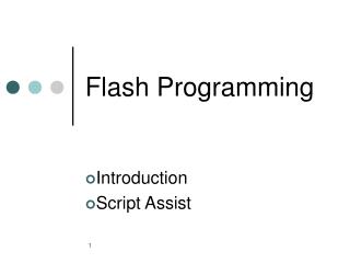
F281x Boot-SCIA Flash Programming
F281x Boot-SCIA Flash Programming. Jeff Stafford Application Report. 28x CPU. Entry Point. Unsecured RAM. PC or ICT. CKFA. RS-232. SCI. Boot-ROM. Step 1 Transfer CFKA to Unsecured RAM LOAD Addresses. Boot-ROM code controls 28x CPU


F281x Boot-SCIA Flash Programming
E N D
Presentation Transcript
F281x Boot-SCIA Flash Programming Jeff Stafford Application Report
28x CPU Entry Point Unsecured RAM PC or ICT CKFA RS-232 SCI Boot-ROM Step 1Transfer CFKA to Unsecured RAM LOAD Addresses • Boot-ROM code controls 28x CPU • Boot-ROM SCI-A code transfers CKFA to LOAD addresses in unsecured RAM • Program Counter set to CKFA entry point when transfer is complete
28x CPU Secured RAM Unsecured RAM PC or ICT RS-232 SCI Boot-ROM Step 2CKFA Unlocks CSM and Transfers to RAM RUN Addresses • CKFA in unsecured RAM controls 28x CPU • CKFA unlocks CSM • CKFA copies itself from LOAD addresses to RUN addresses in secured RAM
28x CPU Secured RAM RAM Buffer #1 RAM Buffer #2 PC or ICT AppCode RS-232 SCI Boot-ROM Step 3CKFA Transfers AppCode to RAM Buffer #1 • CKFA in secured RAM controls 28x CPU • CKFA uses SCI-A to transfer 4KW of AppCode to RAM Buffer #1
28x CPU Secured RAM Flash RAM Buffer #1 RAM Buffer #2 PC or ICT AppCode RS-232 SCI Boot-ROM Step 4CKFA Starts Programming Flash • CKFA in secured RAM controls 28x CPU • CKFA programs flash with RAM Buffer #1 contents • CKFA transfers next 4KW of AppCode to RAM Buffer #2
28x CPU Secured RAM Flash Entry Point 0x3F7ff6 RAM Buffer #1 RAM Buffer #2 PC or ICT RS-232 SCI Boot-ROM Step 5Flash Programming Completed • Device is reset, setting program counter = 0x3F7FF6 • AppCode in flash controls 28x CPU • All RAM available for AppCode use • At 57600 bps, 64 KW program time = 24 sec
Emulated ICT (281x eZdsp) F281x Target 28x CPU 28x CPU RAM (ICT) RAM (CKFA) Flash Flash (AppCode) External RAM (AppCode) PC RS-232 Internal RAM (CKFA) RAM Buffer #1 SCIB CKFA and AppCode RAM Buffer #2 SCIA Boot-ROM SCIA Boot-ROM CKFA and AppCode Emulated ICT Flash Programming • CKFA and AppCode Transfer to Emulated ICT RAM by RS-232 • CKFA Transfer to Target RAM by Boot-ROM Controlled SCI • AppCode Transfer to Target Flash by CKFA Controlled SCI • At 1.875 Mbps, 64 KW program time = 1.4 sec
Emulated ICT - HW Hardware: • (2) F2812 eZdsps From Spectrum Digital • RS-232 Interface from Link Research • JTAG Emulator from Spectrum Digital EICT - Target Direct SCI Connection F281x Target PC RS-232 Interface CCS JTAG Interface Emulated ICT (EICT) Software: • PC = HyperTerminal • EICT = Application Report EICT SW • Target = Application Report CKFA SW