Download
1 / 14
160 likes | 778 Views
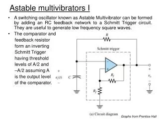
Astable multivibrators I. A switching oscillator known as Astable Multivibrator can be formed by adding an RC feedback network to a Schmitt Trigger circuit. They are useful to generate low frequency square waves. The comparator and feedback resistor form an inverting

E N D
Astable multivibrators I • A switching oscillator known as Astable Multivibrator can be formed by adding an RC feedback network to a Schmitt Trigger circuit. They are useful to generate low frequency square waves. • The comparator and feedback resistor form an inverting Schmitt Trigger having threshold levels of A/2 and –A/2 assuming A is the output level of the comparator. Graphs from Prentice Hall
Astable multivibrators II • The operation of the Astable Multivibrators can be described as follows: at time 0, the initial voltage on the capacitor is 0, assuming the initial output voltage is +A (A is the level of the comparator output). Thus, initially the capacitor is charged through the resistor R toward +A. However, when the capacitor voltage reaches A/2, the output voltage rapidly switches to –A. • Then the capacitor starts to discharge, once the voltage drops below –A/2, the output again switches back to A. Thus, the capacitor voltage cycles back and forth between A/2 and –A/2. • Voltage across capacitor resembles Triangular wave and comparator output voltage is symmetrical square wave.
Astable multivibrators III • The period and frequency of the output square waveform can be determined by analyzing the transient response of the RC feedback network. • The frequency of oscillation for the Astable Multivibrator shown before is • In real circuit design, several non-idealities related to the comparator can affect the frequency, such as the propagation delay of the comparator and bias current effects. • To minimize the bias current effects, we usually need to make sure that the smallest current charging to the capacitor should be much larger than the bias current, for example, a few hundred times.
The 555 Timer I • The 555 timer analog IC (Integrated Circuit) is very economical and convenient for use in mutivibrator circuits since few external components are required.
The 555 Timer II • The 555 timer IC has two comparator, one SR flip-flop and one switching BJT transistor. • Power supply voltage Vcc is applied to a series of three resistors so that almost 1/3Vcc and 2/3Vcc is established. • The reset, threshold and trigger control the state of the flip-flop. If reset is low, Q output is low regardless of the input applied, and transistor is saturated in this case. So, reset has the highest priority in setting Q. When reset is high (connected to Vcc) it does not affect the output Q. • If the trigger input is lower than 1/3Vcc, then the comparator output is high, setting Q to high and transistor is off. • If the threshold input becomes higher than 2/3Vcc, then the output of the comparator is high, resetting Q to low and transistor is in saturation.
The 555 Monostable Multivibrator • A Monostable Multivibrator is a circuit that produces an output pulse of fixed duration each time the input of the circuit is triggered. This is useful in producing timing signals.
The 555 Astable Multivibrator • An Astable Multivibrator can be formed by adding two resistors and a capacitor to the 555 timer.
Half-wave Precision Rectifiers I • Precision half-wave and full-wave rectifiers are very useful in signal processing applications, such as converting AC signal to DC signal. • Consider positive input, the output voltage of X1 becomes positive, and the diode is forward biased. Due to feedback connection, the input voltage of X1 is forced to 0. Then, from the voltage follower X2, input voltage appears at the output. • Consider negative input, output voltage of X1 becomes negative, and diode is reverse biased. So, no current flow on R (feedback path of X1 is not in effect). Voltage at inverting terminal of X1 is set to 0, which appears at the output voltage of X2 as 0.
Half-wave Precision Rectifier II • Error due to offset voltage and bias current in Half-wave precision rectifier circuit usually are on the order of 1-2% of the peak voltage (e.g, the input voltage is a few hundred milli-volts) • Typical problems comes from non-zero reverse-biased diode current, input bias current of OpAmp, offset voltage of the OpAmp, slew-rate limiting when the output needs to change from 0 to negative extreme and negative extreme to positive value.
Improved Half-wave Precision Rectifier • A second diode D2 is connected to keep the output voltage of X1 from being driven to its negative extreme. • X2 is still a voltage follower with a low output impedance. • The output signal is an inverted version of the half-wave rectified input signal • The circuit amplifiers the signal by the gain factor of R2/R1.
Precision Full-wave Rectifier • The circuit can be considered to consist of two parts, a half-wave rectifier and a summer circuit. • At the positive cycle of Vin, the output voltage at point A is a inverted version of Vin. • At the negative cycle, the voltage at A is 0.
Precision peak detector • An ideal peak detector should produces a DC output waveform that is equal to the preceding peak value of the input signal • If the difference is positive, OpAmp produces current to charge capacitor. • If the difference is negative, feedback path is broken and the voltage on the capacitor remains.
Sample and hold circuit • A clock MOS acts as a switch to control the state of operation, sampling state and hold state • Due to slew rate limitation of OpAmp, output takes some time to settle to the value close to the input voltage in the sampling state
Precision clamp circuit • Clamp circuit is to add a DC voltage to the input so that the sum is never negative. • OpAmp X2 is used as a voltage follower so that current could be delivered to the load without affecting the charge on the capacitor • If inverting input of X1 is positive, output of X1 is in negative extreme and diode is off. But voltage capacitor remains steady. • If inverting input of X1 is negative, diode is on and capacitor take the voltage of vin