Download
1 / 1
10 likes | 160 Views
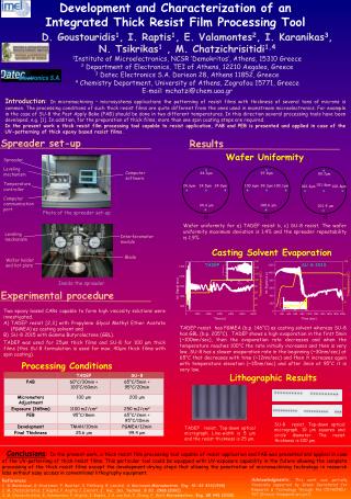
Development and C haracterization of an I ntegrated T hick R esist F ilm P rocessing T ool. D. Goustouridis 1 , I. Raptis 1 , E. Valamontes 2 , I. Karanikas 3 , N. Tsikrikas 1 , M. Chatzichrisitidi 1,4 1 Institute of Microelectronics, NCSR ‘ Demokritos ’, Athens, 15310 Greece

E N D
Development and Characterization of an Integrated Thick Resist Film Processing Tool D. Goustouridis1, I. Raptis1, E. Valamontes2, I. Karanikas3, N. Tsikrikas1 , M. Chatzichrisitidi1,4 1Institute of Microelectronics, NCSR ‘Demokritos’, Athens, 15310 Greece 2 Department of Electronics, TEI of Athens, 12210 Aegaleo, Greece 3Datec Electronics S.A. Dorieon 28, Athens 11852, Greece 4 Chemistry Department, University of Athens, Zografou 15771, Greece E-mail: mchatzi@chem.uoa.gr Introduction: In micromachining – microsystems applications the patterning of resist films with thickness of several tens of microns is common. The processing conditions of such thick resist films are quite different from the ones used in mainstream microelectronics. For example in the case of SU-8 the Post Apply Bake (PAB) should be done in two different temperatures. In this direction several processing tools have been developed, e.g. [1]. In addition, for the preparation of thick films, more than one spin coating steps are required. In the present work a thick resist film processing tool capable to resist application, PAB and PEB is presented and applied in case of the UV-patterning of thick epoxy based resist films. Spreader set-up Experimental procedure Results Wafer Uniformity Spreader Leveling mechanism Computer software Temperature controller Computer communication port 97.9μm 99.7μm 24.3μm 101.8μm a) b) c) 102.3μm 100.6μm 99.3μm 100.1μm 102.8μm 24.6μm 24.5μm 24.9μm Wafer uniformity for a) TADEP resist b, c) SU-8 resist. The wafer uniformity maximum deviation is 1.4% and the spreader repeatability is 1.9% Leveling mechanism Interferometer module 101.9 μm 100.6 μm 24.6 μm Casting Solvent Evaporation Blade Wafer holder and hot plate TADEP SU-8 2015 • Two epoxy based CARs capable to form high viscosity solutions were investigated. • TADEP resist [2,3] with Propylene Glycol Methyl Ether Acetate (PGMEA) as casting solvent and • SU-8 2015 with Gamma Butyrolactone (GBL). • TADEP was used for 25μm thick films and SU-8 for 100 μm thick films (this SU-8 formulation is used for max. 40μm thick films with spin coating). TADEP resist has PGMEA (b.p. 146°C) as casting solvent whereas SU-8 has GBL (b.p. 205°C). TADEP shows a high evaporation in the first 5min (~100nm/sec), then the evaporation rate decreases and when the temperature reaches 100°C the rate initially increases and then is very low. SU-8 has a slower evaporation rate in the beginning (~30nm/sec) at 65°C that decreases with time (~12nm/sec) and then it increases again with temperature elevation (~35nm/sec) and after 3min at 95°C it is very low. Processing Conditions Lithographic Results SU-8 resist. Top-down optical micrograph. 10 μm squares and circle diameter. The resist thickness is 100 μm. TADEP resist. Top-down optical micrograph. Line-width is 5 μm and the resist thickness is 25 μm. Conclusions: In the present work, a thick resist film processing tool capable of resist application and PAB was presented and applied in case of the UV-patterning of thick resist films. This particular tool could be equipped with UV-exposure capability in the future allowing the complete processing of the thick resist films except the development-drying steps that allowing the penetration of micromachining technology in research labs without easy access in conventional lithography equipment. Acknowledgments: This work was partially financially supported by Greek Secretariat for Research & Technology through the 05-NONEU-467 (Greece-Singapore project). • References • G. Bleidiessel, G. Gruetzner, F. Reuther, S. Fehlberg, B. Loechel, A. MaciossekMicroelectron. Eng. 41-42 433(1998) • 2. M. Chatzichristidi, I. Raptis, P. Argitis J. Everett, J. Vac. Sci. Technol. B 20, 2968 (2002) • 3. M. Chatzichristidi, E. Valamontes, P. Argitis, I. Raptis, J.A. van Kan, F. Zhang, F. Watt Microelectron. Eng. 85 945 (2008)