JFET: Introduction, Types, and Characteristics
Learn about Junction Field Effect Transistor (JFET), its types, comparison with BJT, advantages, disadvantages, control mechanisms, and characteristic curves. Understand transfer characteristics and exercises on JFET operation.

JFET: Introduction, Types, and Characteristics
E N D
Presentation Transcript
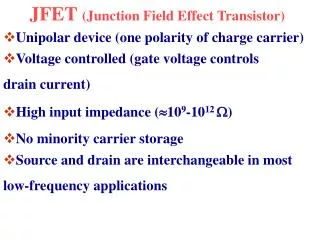
JFET Junction Field Effect Transistor
Introduction (FET) • Field-effect transistor (FET) are important devices such as BJTs • Also used as amplifier and logic switches • What is the difference between JFET and BJT?
Types of Field Effect Transistors (The Classification) • JFET MOSFET(IGFET) n-Channel JFET p-Channel JFET FET Enhancement MOSFET Depletion MOSFET n-Channel DMOSFET p-Channel DMOSFET n-Channel EMOSFET p-Channel EMOSFET
Introduction.. (Advantages of FET over BJT) • High input impedance (M)(Linear AC amplifier system) • Temperaturestable than BJT • Smaller than BJT • Can be fabricated with fewer processing • BJT is bipolar – conduction both hole and electron • FET is unipolar – uses only one type of current carrier • Less noise compare to BJT • Usually use as an Amplifier and logic switch
Disadvantages of FET • Easy to damage compare to BJT
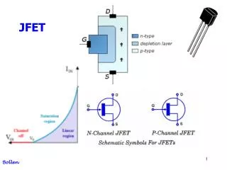
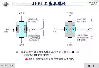
Junction field-effect transistor.. • There are 2 types of JFET • n-channel JFET • p-channel JFET • Three Terminal • Drain – D • Gate -G • Source – S
Drain Drain Gate Gate Source Source SYMBOLS n-channel JFET p-channel JFET
N-channel JFET • N channel JFET: • Major structure is n-type material (channel) between embedded p-type materialto form 2 p-n junction. • In the normal operation of an n-channel device, the Drain (D) is positive with respect to the Source (S). Current flows into the Drain (D), through the channel, and out of the Source (S) • Because the resistance of the channel depends on the gate-to-source voltage (VGS), the drain current (ID) is controlled by that voltage
P-channel JFET • P channel JFET: • Major structure is p-type material (channel) between embedded n-type materialto form 2 p-n junction. • Current flow : from Source (S) to Drain (D) • Holes injected to Source (S) through p-type channel and flowed to Drain (D)
JFET Characteristic for VGS = 0 V and 0<VDS<|Vp| • To start, suppose VGS=0 • Then, when VDS is increased, ID increases. Therefore, ID is proportional to VDS for small values of VDS • For larger value of VDS, as VDS increases, the depletion layer become wider, causing the resistance of channel increases. • After the pinch-off voltage (Vp) is reached, the IDbecomes nearly constant (called as IDmaximum, IDSS-Drain to Source current with Gate Shorted)
JFET for VGS = 0 V and 0<VDS<|Vp| Channel becomes narrower as VDS is increased
ID versus VDS for VGS = 0 V and 0<VDS<|Vp| JFET Characteristic Curve
JFET for (Application of a negative voltage to the gate of a JFET)
JFET Characteristic Curve.. • For negative values of VGS, the gate-to-channel junction is reverse biased even with VDS=0 • Thus, the initial channel resistance of channel is higher. • The resistance value is under the control of VGS • If VGS = pinch-off voltage(VP) • The device is in cutoff (VGS=VGS(off) = VP) • The region where ID constant – The saturation/pinch-off region • The region where ID depends on VDS is called the linear/ohmic region
p-Channel JFET characteristics with IDSS= 6 mA and VP = +6 V.
Transfer Characteristics • The input-output transfer characteristic of the JFET is not as straight forward as it is for the BJT. In BJT: • IC= IB • which is defined as the relationship between IB (input current) and IC (output current).
Transfer Characteristics.. In JFET, the relationship between VGS (input voltage) and ID (output current) is used to define the transfer characteristics. It is called as Shockley’s Equation: The relationship is more complicated (and not linear) As a result, FET’s are often referred to a square law devices VP=VGS (OFF)
Transfer Characteristics… • Defined by Shockley’s equation: • Relationship between ID and VGS. • Obtaining transfer characteristic curve axis point from Shockley: • When VGS = 0 V, ID = IDSS • When VGS = VGS(off) or Vp, ID = 0 mA
Transfer Characteristics JFET Transfer Characteristic Curve JFET Characteristic Curve
Exercise 1 Sketch the transfer defined by IDSS = 12 mA dan VGS(off) = - 6
Exercise 1 Sketch the transfer defined by IDSS = 12 mA dan VGS(off) = Vp= - 6 IDSS VGS =0.3VP IDSS/2 VGS =0.5VP IDSS/4
Exercise 2 Sketch the transfer defined by IDSS = 4 mA dan VGS(off) = 3 V
Exercise 2 Sketch the transfer defined by IDSS = 4 mA dan VGS(off) = 3V IDSS IDSS/2 IDSS/4 VP VGS =0.3VP VGS =0.5VP
Answer 2 Answer 2