Download
1 / 39
400 likes | 447 Views
Explore the advancements in pixel detector technology from Timepix3 to Timepix4 and beyond, focusing on hybrid silicon pixel detectors, counting electronics, sensor materials, and through-silicon via processing. Learn about key collaborations and the potential future developments in this field.

E N D
Moving from Timepix3 to Timepix 4 and beyond M. Campbell1, J. Alozy, R. Ballabriga, N. Egidos, J. Fernandez, E.H.M. Heijne, I. Kremastiotis, X. Llopart, T. Poikela, V. Sriskaran, and L.Tlustos CERN, PH Department 1211 Geneva 23 Switzerland 1Honorary Professor at Glasgow University
The Medipix3 Collaboration (est. 2005) • University of Canterbury, Christchurch, New Zealand • CEA, Paris, France • CERN, Geneva, Switzerland, • DESY-Hamburg, Germany • Albert-Ludwigs-Universität Freiburg, Germany • University of Glasgow, Scotland, UK • Leiden University, The Netherlands • NIKHEF, Amsterdam, The Netherlands • Mid Sweden University, Sundsvall, Sweden • IEAP, Czech Technical University, Prague, Czech Republic • ESRF, Grenoble, France • Universität Erlangen-Nurnberg, Erlangen, Germany • University of California, Berkeley, USA • VTT, Information Technology, Espoo, Finland • KIT/ANKA, Forschungszentrum Karlsruhe, Germany • University of Houston, USA • Diamond Light Source, Oxfordshire, England, UK • Universidad de los Andes, Bogota, Colombia • University of Bonn, Germany • AMOLF, Amsterdam, The Netherlands • Technical University of Munich, Germany • Brazilian Light Source, Campinas, Brazil
The Medipix4 Collaboration (est. 2016) CEA, Paris, France CERN, Geneva, Switzerland, DESY-Hamburg, Germany Diamond Light Source, Oxfordshire, England, UK IEAP, Czech Technical University, Prague, Czech Republic IFAE, Barcelona, Spain JINR, Dubna, Russian Federation NIKHEF, Amsterdam, The Netherlands University of California, Berkeley, USA University of Houston, USA University of Maastricht, The Netherlands University of Canterbury, New Zealand University of Oxford, England, UK University of Geneva, Switzerland University of Glasgow, Scotland, UK
Hybrid Silicon Pixel Detectors Standard CMOS can be used allowing on-pixel signal processing Sensor material can be changed (Si, GaAs, CdTe..)
Gas detector readout - InGrid Semiconductor detector is replaced with charge amplification grid Permits lower energy events to be detected NB: GEM foils may be used in place of the InGrid foils
Hybrid Pixel Detector – Counting Electronics Voltage Open shutter Close shutter Qin ~ 4000e- threshold ~ 600e- Threshold Noise hit free imaging Amplifier output noise ~ 60e- rms Time
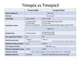
Timepix3 Specs * Thanks to V. Gromov, et al. Nikhef, C. Brezina et al., Bonn
Timepix3 Specs * Thanks to V. Gromov, et al. Nikhef, C. Brezina et al., Bonn
Timepix3 Specs * Thanks to V. Gromov, et al. Nikhef, C. Brezina et al., Bonn
Timepix3 Specs * Thanks to V. Gromov, et al. Nikhef, C. Brezina et al., Bonn
Timepix3 Specs * Thanks to V. Gromov, et al. Nikhef, C. Brezina et al., Bonn
Timepix3 Specs * Thanks to V. Gromov, et al. Nikhef, C. Brezina et al., Bonn
Pixel Operation in TOA & TOT Tpeak < 25ns Preamp Out Disc Out Pixel Readout Starts (475ns→ 19 clock cycles) Clk (40MHz) Global TOA (14-bit) VCO Clk (640MHz) TOA (14-bit) 16382 16383 16384 0 1 2 3 4 TOT Clk (40MHz) FTOA (4 bits)=7 X 16383 TOA (14 bits)=16383 TOT (10 bits) =4
Trigger-less event-by-event data drivenand zero-supressed readout • Achievable count rate: • uniformly distributed events → ~40 Mhits/s/cm2 @5.12Gbps • Full matrix readout: ~800 µs @5.12Gbps Acquisition time Shutter Qin DataOut 48bit 48bit 48bit 48bit 48bit 48bit ChipID [32b] 0x71 0xB0 Address[16-bit] Data[28-bits] 0xB Data Packet (48 bits) End of Command (48 bits)
Test with 120GeV/c Pion Track 60 deg p+ in n Si sensor 500mm thick Vbias = 130V Colour (and diameter) indicate charge Measured z resolution ~50mm Slide courtesy of B. Bergmann, S. Pospisil, IEAP, CTU, Prague
Velopix (2016) 14140 µm Sensitive Area (14080 µm) 16600 µm X. Llopart
5.12 Gbps Velopix High Speed link Full link 3-chip module with all links at 5.12 Gbps over a 1m copper line
Tiling larger areas Sensor Single chip assembly ASIC
Tiling larger areas– present day solution ASIC Ladder – n x 2 ASIC
Tiling larger areas - TSVs at periphery TSVs for IO eliminate wire bonding reducing dead area
Tiling larger areas - TSVs within pixel matrix If IO are distributed within the pixel matric TSVs permit seamless tiling
Tiling larger areas - TSVs within pixel matrix Permits use of single 4-side buttable tiles
Through Silicon Via processing of Medipix3/Timepix3 Through Silicon Vias offer the possibility of creating 4-side buttable tiles 3 projects for been undertaken with LETI - Funding mainly from Medipix3 Collaboration, AIDA and LCD group 2011 - Feasibility of TSV processing on Medipix3 (low yield wafers) 2013 - Proof of yield using Medipix3RX wafers (6 wafers) 2014 - TSV processing of ultra-thin Medipix3/Timepix3 wafers (50mm)
What’s next? • The Medipix4 Collaboration was started in March 2016 • Chips to be fully tile-able on 4-sides – use of Through Silicon Vias (TSV) for I/O • Medipix4 Photon counting spectrometric chip • Will use charge summing and allocation scheme • Multiple thresholds • Pixel pitch varied to match sensor material • Better high count rate performance (aimed at human CT) • Timepix4 • Better timing resolution (~200ps) • Better high count rate performance (TSV) Sensor ASIC PCB
Timepix3 Timepix4 3.5x 33% 8x 10x 2x 8x 16x
Timepix4 Pixel Schematic 1 pixel 8 pixels 32 pixels Front-end Front-end Super pixel SPG 8-bits Leakage Current compensation Counters & Latches 8-bits Clock local ADB Sync Readout Input pad 2.5fF Synchronizer & Clock gating Preamp 8 TestBit MaskBit 14-bits ~50mV/ke- 8-bits VCO @640MHz 4 5-bit Local Threshold 3fF 640MHz X. Llopart Data out to EOC Time stamp clock (40MHz) OP Mode TpA TpB Control voltage Global threshold
Pixel Operation in TOA & TOT [DD] Tpeak < 25ns Preamp Out Disc Out Clk (40MHz) Global TOA (16-bit) VCO Clk (640MHz) TOA (16-bit) FTOA_R (4 bits)=7 FTOA_F (4 bits)=11 TOT Clk (40MHz) UFTOA_Start (4-bits) X 65533 X 0 65534 8 65535 0 1 2 3 4 X. Llopart UFTOA_Stop (4-bits) X 65534 TOA (16 bits)=65534 TOT (10 bits) =4
Timepix4 Floorplan • Chip size 28.16mm x 24.64 mm (no Wirebonds) • 512 x 448 229376 pixels • Pixel size 55µm x 55µm • Analog Periphery (< 800 µm): • BandGap + Temperature sensor • Biasing DACs • Monitoring ADC • Analog supply • Digital supply • 2 x Digital Periphery ( < 400 µm): • 8 x 5.12Gbps serializers (configurable) • PLL(s) • Analog supply • Digital supply • 2 x Pixel matrix (13.28 mm x 24.64mm): • 256 x 448 pixels 55 µm x 51.875 µm • 5.68% smaller than 55 µm x 55 µm • RDL to compensate up to 400 µm X. Llopart
29960 µm Timepix4 Floorplan q TSVs TSVs 13158.4 µm (256 x 51.4 µm) 28160 µm (512 x 55 µm) 24700 µm 24640 µm (448 x 55 µm) X. Llopart WB_BOT (900 um) TSV_BOT (460 um) TSV_TOP (460 um) WB_TOP (900 um) TSV_MID (920 um)
Edge periphery floorplan TSV Dice line • Digital on top design: • Default periphery size is 460.8 µm • Scripted to allow different periphery sizes • IO TSV/WB structure completed • Missing blocks: • 5.12 GbpsSerializer (Nikhef) • SLVS TX (CERN) • WB openings 4x 100x70 µm • Multiple probing pads • TSV M1 octagons of 69 µm • First version of edge routing • 13158.4 x 5.4 µm • Buffer routing between peripheries X. Llopart WB_Periphery (900 µm) Periphery (460.8 µm) Pixel Matrix (256 x 51.4 µm)
TSV (on M1) and BUMPs (on M10) 55 µm 55 µm X. Llopart
Timepix4 IO • 2 peripheries when using Wire-Bonds (WB): TOP, BOT • 3 peripheries when using TSVs: TOP, MID, BOT • General strategy is to allow the control of Timepix4 from any of the 3 peripheries (TOP, MID, BOT): • Non connected control lines will be pulled-up/down internally • All control signals routed to the MID periphery and Or-ed: • E.g. SHUTTER_TOP | SHUTTER_MID | SHUTTER_BOT = SHUTTER • Serial readout (SERIAL_OUT[7:0]) only available through TOP and BOT peripheries • 2 Digital CMOS inputs to be used as coincidence time alignment • TSV pitch 165 µm (3x55) • 147 TSVs in each periphery • 147 WB in TOP and BOT periphery extenders • Submission target date 2019 Q2 X. Llopart
Future developments • Medipix4 chip • 130nm CMOS • More threshold bins • 75 mm pixels • 400 x 400 pixels • Count rate ~ x 5 Medipix2 (human X-ray CT) • VELOpix2 • Possibly 28nm CMOS • Possibly smaller pixels • < 100ps timing bin • High rate capability (~ x10 VELOpix)
Thank you for your attention! Medipix3RX images: S. Procz et al.