Download
1 / 29
290 likes | 310 Views
Discuss several systems built in the past, including the PHENIX experiment Hadron Blind detector digitizer readout system and Data Collection Module upgrade. Also covers electronics for the MicroBooNE Neutrino Liquid Argon TPC Front End Board and future sPHENIX experiment calorimeter electronics. Shares lessons learned in building electronics projects.

E N D
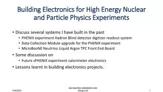
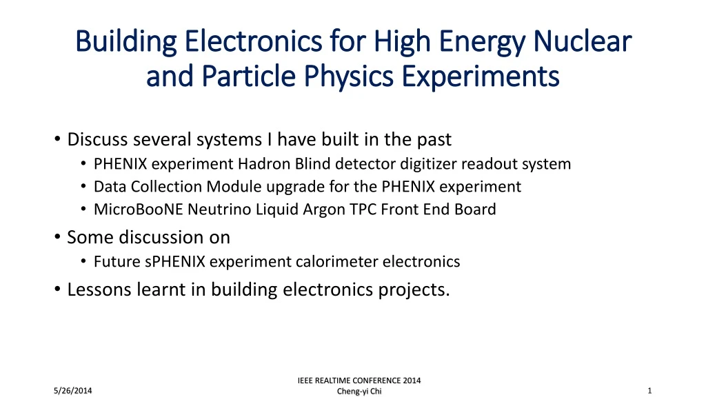
Building Electronics for High Energy Nuclear and Particle Physics Experiments • Discuss several systems I have built in the past • PHENIX experiment Hadron Blind detector digitizer readout system • Data Collection Module upgrade for the PHENIX experiment • MicroBooNE Neutrino Liquid Argon TPC Front End Board • Some discussion on • Future sPHENIX experiment calorimeter electronics • Lessons learnt in building electronics projects. IEEE REALTIME CONFERENCE 2014 Cheng-yi Chi
PHENIX experiment in RHIC at BrookHaven National Lab. Heavy Ion Physics p + p Spin Physics HBD 2006-2009 IEEE REALTIME CONFERENCE 2014 Cheng-yi Chi
PHENIX Online System (upgrade) (baseline) on detector Front-End Module (FEM) L1 trigger Front-End Module (FEM) RHIC clock is about 9.8 MHz depend on collision specs. Level 1 trigger delay is 40 beam crossing L1 trigger rate is 10 KHz. To keep system live time near ~100%, FEMs store 5 L1 triggered events Frontend are built by various groups. DCM & DCM II are used to interface with all the FEMs. (first stage of the event builder) off detector Data Collection Module(DCM) Data Collection Module II(DCM II) JSEB JSEB II Sub-Event Buffer Sub-Event Buffer Ethernet Switch Assembly Trigger processor (ATP) Assembly Trigger processor (ATP) Archive IEEE REALTIME CONFERENCE 2014 Cheng-yi Chi
Mesh HV panel g Triple GEM module with mesh grid Primary ionization HV e- CsI layer Pad readout plane Triple GEM Readout Pads Mylar entrance window Honeycomb panels HV panel HADRON BLIND DETECTOR • Proximity focus Cherenkov counter. (sensitive only to electron) • Use CsI to convert photon to electron. • GEM is used for amplify the electron from CsI. • Measure time and charge • 2006 - 2009 IEEE REALTIME CONFERENCE 2014 Cheng-yi Chi
15 mm 19 mm Preamp (BNL IO-1195) 2304 channels total Charge Preamp with On-Board Cable Driver(IO1195-1-REVA) • Features: • +/- 5V power supply. • 165 mW power dissipation. • Bipolar operation (Q_input = +/- ) • Differential outputs for driving 100 ohm twisted pair cable. • Large output voltage swing -- +/- 1.5V (cable terminated at both ends) • (+/- 3V at driver output) • Low noise: Q_noise = 345e (C_external = 5pF, shaping = .25us) • (Cf = 1pF, Rf = 1meg) • Size = 15mm x 19mm • Preamp output (internal) will operate +/- 2.5V to handle large pile-up. IEEE REALTIME CONFERENCE 2014 Cheng-yi Chi
Use 2MM Hard Metric cable to move signals between preamp/FEM 2mm HM connector has 5 pins per row and 2mm spacing between pins and rows There are two types of cable configuration: *100 ohms parallel shielded cable 50 ohms coaxial cable Signal arrangement S- S+ G S- S+ MERITEC Our choice is This gives us signal density 2mm x 10mm for every 2 signals. Same type of cables will be used for L1 trigger data. IEEE REALTIME CONFERENCE 2014 Cheng-yi Chi
FEM receiver + ADC Preamp Cable driver Differential Receiver ADC FPGA TI ADS5272 Based on AD8138 receiver Unity gain 8 CHANNEL 65 MHz 12 bits ADC (80 TQFP) The +/- input can swing from 1V to 2V, Vcm=1.5V + side 2V, - side 1V -> highest count - side 2V, + side 1V -> lowest count Our +/- input will swing from 1.5 to 2V/ 1.5 to 1V we will only get 11 bits out of 12 bits 16fc will be roughly sitting at 200 count We will run the ADC at 6X beam crossing clock 6X9.4 MHz = 56.4 MHz or ~17.7ns per samples ADC data are serialized LVDS at 12*56.4 MHz= 678 MHz IEEE REALTIME CONFERENCE 2014 Cheng-yi Chi
HBD ADC board We use ALTERA STRATIX II 60 FPGA to receive the 6 ADC’s data (8 channel per ADC) It has 8 SERDES blocks. ALTERA provides de-serializer Mega function block. 6XADC clock SERDES clock data de-serialized as 6 bit 120 MHZ Regroup to 12 bits at 60 MHz , 45 degree phase adjustment step. Timing Margin 270 degree. • The FPGA also provides • L1 delay (up to 240 samples) • 8 events buffer • ADC setting download • Offline slow readback • 7 threshold levels for L1 trigger primitives per channel. ALTERA FPGA ADC Differential receiver 48 channels per board 6U X160 mm size Signals from Preamp IEEE REALTIME CONFERENCE 2014 Cheng-yi Chi
Electronics Rack Pedestal Run Mean(ch) Width s(ch) Channel # Mean(ch) Width s(ch) Channel # IEEE REALTIME CONFERENCE 2014 Cheng-yi Chi
Data Collection Module II (DCM II) • Receives all the data from the upgrade detectors frontend modules • Provide 5 event buffers for the FEMs. • Data transmission time is based on average trigger rate. • to achieve minimum trigger deadtime. • FEM’s data are not compressed. DCM II compresses the raw data and formats the data for the Event builder. • Collects the compressed FEM data to the event builder • Error monitoring. • Provides slow readback path for detector readout without the event builder. IEEE REALTIME CONFERENCE 2014 Cheng-yi Chi
DATA COLLECTION MODULE II (DCM II) detector dependent Test data 32KX32 Dual port Stratix III 1.6 Gbits/sec Optical link 65kx18 FIFO compressor TLK 2501 M U X Interface to the frontend electronics Compress/Merge/5 events bufferError checking data packet Used in VTX (strip and Pixel), FVTX 256X45 Header FIFO busy 80 M words ( 16bits wide) Event number Memory address Word counts (FIFO has more than 16K words) 9bits X 4 at 480 MHz busy 256X45 Header FIFO 1.6 Gbits/sec Optical link 65kx18 FIFO compressor TLK 2501 16Kx32 FIFO Demux Align 9bits X 4 at 480 MHz 32KX32 Dual port Test data hold M U X 64KX32 Dual port Link port Data In/out (LVDS) 16Kx32 FIFO Demux Align 8 1.6 Gbits/sec optical ports per module Individual ports can be enabled or disabled 8 80 MHz 16bits words in 80 MHz 32 bits word out Token In/out 256X60 Header FIFO 16Kx32 FIFO Demux Align detector dependent hold Test data 16Kx32 FIFO Demux Align 32KX32 Dual port 1.6 Gbits/sec Optical link Test data 65kx18 FIFO compressor TLK 2501 M U X 256X45 Header FIFO busy 80 M words ( 16bits wide) Event number Memory address Word counts FPGA Download control/ readback (FIFO has more than 16K words) 9bits X 4 at 480 MHz 48 V on/off busy 256X45 Header FIFO 1.6 Gbits/sec Optical link 65kx18 FIFO compressor TLK 2501 slow control /download 32KX32 Dual port Test data IEEE REALTIME CONFERENCE 2014 Cheng-yi Chi
DCM II DATA FLOW DIAGRAM DCM II DCM II DCM II token,hold data, busy 40 MHz 8 bits data + 2 bits control data, busy token,hold Partition module output data with 2 3.125 Gbits optical link to JSEB module. The hold is returned via optical link. Controller allows us to: Download FPGA code and setup system parameters. Readback system status and provide a data readback path during detector commissioning. Token/demux/align/busy/hold Mux/demux busy Partitioner III controller Buffer Buffer Timing System optical transceiver optical transceiver optical transceiver L1 System optical transceiver optical transceiver optical transceiver optical transceiver buffer buffer buffer buffer JSEB II JSEB II PCI express IP core PCI express IP core IEEE REALTIME CONFERENCE 2014 Cheng-yi Chi
DCM II system first production was done for vertex strip and pixel detector & forward vertex in 2010 DCM modules JSEB II Module DCM crate In PHENIX IEEE REALTIME CONFERENCE 2014 Cheng-yi Chi
MicroBoone Experiment Liquid Argon TPC detector For Neutrino Physics Cryostat: Keeps Ar liquid < 87.3oK Welded p0gg simulation Drift Electronics Platform Cryostat Cryostat IEEE REALTIME CONFERENCE 2014 Cheng-yi Chi
Overall Electronics scheme 8256 Time Projection Chamber wires 32 PMT’s provide a neutrino trigger in time with beam gate Blue Nevis IEEE REALTIME CONFERENCE 2014 Cheng-yi Chi
FEM Concept Build a system that can take both triggered data (lossless compression) and continuous recording (lossy compression). System is running continuously. Record both Neutrino events / SuperNova events. The FEM (frontend module) organizes ADC data as frames. Grouping/processing of the frame depends on whether there is trigger or not. The neutrino event will consist of several frames. If no trigger, the frames will be continuously recorded. Once the data is processed, the events will flow to the computer in separate paths. Keep neutrino and SuperNova events’ flows as independent as possible easier to prioritize the event flow. IEEE REALTIME CONFERENCE 2014 Cheng-yi Chi
Data Sample memory Arrange the sample memory into 4 frames Each frame can store up 2ms of data (currently set at 1.6ms) Sampling speed set a 2MHz maximum 2MHz* 64 channel =128MHz 16 bits word 64 MHz 32 bits word (2 ADC’s / word) (sampling frequency drive memory speed) Use alternate cycle for write/read (100% live) frame write pointer read pointer frame frame frame trigger Neutrino M U X 128MHz 1M X 36 SRAM ADC decimation supernova ADC decimation Frame Data 16 MHz ADC 2 MHz sample Time The system clock is free running. It is not synch with the accelerator. ADC decimation 16MHZ ADC clock ADC decimation 16 MHz clock FPGA PLL r/w address Downsampling + anti-aliasing filter Init(/Run) trigger IEEE REALTIME CONFERENCE 2014 Cheng-yi Chi Frame synch 128 MHz Frame buffer clock
TPC DATA PROCESSING Event number Word count memory address Huffman code by (Jin-Yuan Wu) Difference 0 assign code 0 +1 assign code 1 -1 assign code 2 etc 3 16 bits word 2 24 bits word 2 30 bits ECC words (5+1 parity) Slow Control readback DRAM Pointer FIFO 2 sample per cycles Read/write every other cycle SRAM Neutrino token Has priority over Supernova token Pre-buffer 16KX40 FIFO Hamming code/packing LINK Neutrino Token Neutrino compressor Neutrino Data header demux /align /decimation Frame generator SRAM write/read Neutrino Path Link data ADC SuperNova Path SuperNoa Data header LINK SuperNovacompressor fake data SuperNova Token Pre-buffer 16KX40 FIFO Hamming code/packing Need compression factor 20 to 80 Probably will use some threshold plus Huffman coding (remove as much noise as possible) trigger DRAM Pointer FIFO Slow Control readback Read has priority over Write on DRAM access DATA FLOW IEEE REALTIME CONFERENCE 2014 Cheng-yi Chi
Pack 2 samples into one word PMT DATA PROCESSING PMT DATA PROCESSING Frame number sample number packetize 1KX33 FIFO PMT shaper ADC S R A M wr Neutrino gates 64 MHz clock Post-pre compare Beam Cosmic Michel diff(i) = Ph(i+n)- ph(i) diff(i) > Threshold(ch) Trigger Logic Trigger Module 40 channels PH(max) & width NHITS, PHSUM diff(i) > Threshold(ch) diff(i) = Ph(i+n)- ph(i) 64 MHz clock Neutrino gates Post-pre compare PMT shaper ADC packetize 1KX33 FIFO DATA FLOW PMT data is sampled at 64 MHz. It is not possible to write all this data into SRAM with the available frame space Only keep the data associated with discriminator firings (neutrino data + cosmic rays). (* data compression before buffer*) IEEE REALTIME CONFERENCE 2014 Cheng-yi Chi
We went through two production cycle: 1) For Microboone ( early last year) 147 FEM modules 5 PMT ADC modules and supporting modules for 10 crates 2) For LANL (late last year) 54 FEM modules and supporting modules for 5 crates PMT ADC + FEM board SRAM Stratix III DRAM FEM Board TPC ADC + FEM board IEEE REALTIME CONFERENCE 2014 Cheng-yi Chi
The sPHENIX Detector Solenoid Magnet HCAL EMCAL Solenoid VTX PS 1-40 The SuperPHENIX Upgrade of the PHENIX Experiment at the Relativistic Heavy Ion Collider M. Purschke IEEE REALTIME CONFERENCE 2014 Cheng-yi Chi
Original Concept: Optical Accordion (EM section) Accordion design similar to ATLAS Liquid Argon Calorimeter Readout Towers Fibers Plates Particle • Accordion prevents channeling • and allows readout on the front • or back of the absorber stack • Can make projective in r-f by • tapering thickness of tungsten • plates • Can make projective in h by • fanning out fibers • Oscillations must be kept small • because of minimum bending • radius of fibers and plates Want to be projective in both r-f and h IEEE REALTIME CONFERENCE 2014 Cheng-yi Chi
HCAL Readout Scintillating tiles with WLS fibers embedded in grooves Fibers read out with SiPMs T 2x11 scintillator tile shapes 8 readout fibers per tower Outer readout SiPMs + mixers 2x11 segments in h (Dh =0.1) 64 segments in f (Df =0.1) 1408 x 2(inner,outer) = 2816 towers Inner readout (~10x10 cm2) Outer Inner IEEE REALTIME CONFERENCE 2014 Cheng-yi Chi
Discrete Preamp Cd = 640pF for dual SiPM, Ist stage Av = 65, multi-pole differential output filter IEEE REALTIME CONFERENCE 2014 Cheng-yi Chi
sPHENIX Calorimeter digitizer electronics Mini SAS • Similar to HBD ADC system. • We will use 14 bits ADC instead of 12 bits ADC while maintaining speed at 60 MHz • Including offset to deal with signal only swing one side • Better cables and connector arrangement. • Instead of ~ 2400 channel 30,000 channel • 48 channels/board 64 channel board • Add optical output for L1 trigger primitives output. • Add secondary path for short trigger summary output. • Instead of using LVDS to multiplex data between modules, we will use multiple Gbits transceivers to pass the data between the modules. IEEE REALTIME CONFERENCE 2014 Cheng-yi Chi
Cost & Schedule • Understand the major cost of the system. • Most of the majors components, ADC, FPGA etc. Past printed circuit board and assembly cost. • Estimate the cost of the system within some margins. • You have to cover some unknown cost that could happen down the road. • Boss always pushes initial cost lower and will be much more unhappy if you have to ask more fund at the tail end of the project: • This is the time when the project has less money and less freedom of where to spend it. • Estimate the schedule conservatively • Prototype has lots of unknown both technically or surprise from detector group. • Testing always takes longer • Production has to deal with real world schedule, like part shortage…. • Surprise in the production.. IEEE REALTIME CONFERENCE 2014 Cheng-yi Chi
Design Specification • Carefully discuss the specification of the readout electronics • In the proposal stage, detector specification almost always idealized. • Always try to build more than they ask. • Occupancy of the detectors are under-estimated. • Don’t be surprised, if they come back ask for more after the initial design is done. • Try to have a conservative design. • Don’t under estimate number of prototype modules needed • Before production, prototypes are needed for detector group, DAQ group, your lab. • Don’t give out the prototype system freely. • It needs lot of support. • PCB manufacture produce boards with a minimum lot. The cost of one board and 10 boards may be exactly the same. • For a small system, the extra boards could be used for the productions if it is successful. IEEE REALTIME CONFERENCE 2014 Cheng-yi Chi
Prototype • We have done the last 4 readout systems where the prototype is the production design with only pre-cautionary modification except for 1 module. This is achieved by • Don’t fabricate anything till all the boards are designed. • Finish the FPGA design enough till all the I/O pins are done. • Work out the testing method and all testing features that are needed. • Our engineers design/layout the board. I independently check the board. • I normally read all the data sheets carefully. Check the layout compared to the data sheets. • Check the FPGA pin out against the layout. Read the small footprints. • Check the mechanical dimensions. Mounting holes placement. • Get parts. Put parts on the layout printout to check footprint. • Figure out the power up state of the board. • Check the pull up and pull down of lines critical during the startup. • Talk to board assembler about the component placement restrictions near the connectors. • When the design is revised, re-check everything again. • Look at the checkplot. IEEE REALTIME CONFERENCE 2014 Cheng-yi Chi
The past decade • Because we only work on small projects without extended reviews. It allows us to use up-to-date technologies. • We spend most of time just on building electronics and make sure it will run smoothly in the experiments. • It is a continuous design/prototype/fabrication cycle during the past decade. • Helped by the our engineers, we have built 4 readout systems for PHENIX and MicroBooNEexperiements. • MicroBoone will fill the tank with liquid Argon sometime around the summer. • We will proceed to prototype the sPHENIX EM & Hadron calorimeters digitize system in the next 1.5 years. IEEE REALTIME CONFERENCE 2014 Cheng-yi Chi