Download
1 / 1
10 likes | 147 Views
A 10-bit 40MS/ s pipelined ADC in a 0.13µ m CMOS process. F. 1. F. F. 2. 2. F. 0. TWEPP – 09 Paris 21-25 September 2009 Hugo França Santos (CERN). F. F. 1. 1.

E N D
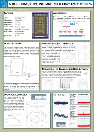
A 10-bit 40MS/s pipelined ADC in a 0.13µm CMOS process F 1 F F 2 2 F 0 TWEPP – 09 Paris 21-25 September 2009 Hugo França Santos (CERN) F F 1 1 Features Process IBM 8RF_DM 0.13µm Supply Single 1.5V Sampling Rate 10 to 40MS/s DNL @ 40MS/s< 0.6 LSB INL @ 40MS/s< 0.8 LSB ENOB @ 40MS/s 9.1-bit, FIN = 1MHz 8.6-bit, FIN = 20MHz SFDR @ 40MS/s min 65dB, FIN = 1 to 20MHz Power/Channel 34 mW @ 40MS/s 26 mW @ 20MS/s ADC Die Area 0.7 mm2 Prototype Die Area 3.8 mm2 Architecture Pipelined topology with eight 1.5-bit stages followed by a 2-bit stage, since it offers the best compromise in terms of power and area for the speed and resolution required. Double Sampling The multiplying digital-to-analogue converters (MDACs) were implemented with switched capacitors using the double sampling principle that removes the need of a sampling phase where the amplifier not needed. This technique relaxes the operational amplifiers speed requirement to half of the one in a conventional implementation, consequently a reduction of around 50% of the power consumption is achieved. An important draw-back of the double sampling implementation is the introduction of a different timing skew between even and odd samples. This problem was overcome by the insertion of a synchronization switch that makes the sampling circuit skew insensitive . Optimum sub-ADC Thresholds In a 1.5-bit sub-ADC, the standard threshold levels are ± ¼ VREF, however the levels that minimize the errors due to capacitor mismatch are ± ½ VREF. Unfortunately these levels are impractical since they would require extremely high precision comparators. A good trade-off for minimizing these errors and still allow the use of low precision comparators is to set the threshold levels to± ⅜ VREF, this reduces error caused by capacitor mismatches by 12.5% in each stage, accumulating a total improvement of 24.9% in a9-stage configuration. F1 C12 C11 F1 F2 F1 VIN(i) F2 VDAC C22 F0 Optimization of Transmission Gate Switches C21 VOUT(i) The use of transmission gate switches for sampling high bandwidth signals is critical in a low voltage design because of the non-linear trait of their ON resistance. The use of low-Vt transistors with an optimized length enabled a considerable increase of the linearity of the switches and the reduction of the highest harmonic from -68 to -77dB (-72dB in the worst corner). FS Operational Amplifier Test Results OUTPUT SPECTRUM 1MHz Test Conditions Fs = 40 MS/s Fin = 1.0071MHz N = 32768 Test Results ENOB = 9.07 SINAD = 56dB SFDR = 75dB THD = -70dB The selected topology for the operational amplifier is a 2-stage OTA with PMOS inputs, gain boosting in the first stage, continuous-time common mode feedback sensed with a resistor/capacitor and biased with an externally regulated Beta-multiplier circuit. The frequency compensation is both indirect and direct with the nulling resistor. OUTPUT SPECTRUM 10MHz Test Conditions Fs = 40 MS/s Fin = 9.9915MHz N = 32768 Test Results ENOB = 8.80 SINAD = 55dB SFDR = 65dB THD = -64dB Test Conditions Fs = 40 MS/s Fin = 19.989MHz N = 32768 Test Results ENOB = 8.63 SINAD = 54dB SFDR = 68dB THD = -65dB OUTPUT SPECTRUM 20MHz Hugo.Franca.Santos@cern.ch