Download
1 / 20
200 likes | 239 Views
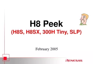
H8 Peek (H8S, H8SX, 300H Tiny, SLP). February 2005. H8 CPU Core Road Map. 1) Superior CPU performance at the same frequency 2) Superior Instruction code efficiency 3) H8 devices are compatible at the object code level. Enhanced Bus width to 32bit. 32-. bit. H8SX. Bus:32bit. (4GB).

E N D
H8 Peek(H8S, H8SX, 300H Tiny, SLP) February 2005
H8 CPU Core Road Map 1) Superior CPU performance at the same frequency 2) Superior Instruction code efficiency 3) H8 devices are compatible at the object code level Enhanced Bus width to 32bit 32- bit H8SX Bus:32bit (4GB) fmax: 50MHz 1 Instruction/1 state X : eXtension , eXpansion H8S 16 MB Linear Addressing Enhanced external mode 16- bit fmax: 33MHz Bus:16bit H8/300H (16MB) fmax: 25MHz 300 300 H H8S H8SX Original Core Basic instruction execution state 2 state 1 state 8- bit H8/300 8 bit 16 bit 32 bit Data Bus width Bus:8bit Number of instructions 57 62 69 87 (64kB) fmax: 16MHz Number of addressing modes 8 8 8 11 Address space 64 KB 16 MB 4 GB
H8/H8S/H8SX Family Features Products Series Process Technology Maximum frequency Target segments Development & Sales strategy Features 0.18um (F-MONOS) f=33MHz => 48MHz Printer, ODD Auto H8SX 32bit, CISC A.S.S.P. 16bit,Multiplier S-DRAM I/F H8S/2600 0.5 - 0.18um f=33MHz Printer A.S.S.P. H8S/2500 16 bit, CAN, IE 0.18um f=25MHz Car Audio A.S.S.P. 16 bit, Multiplier DDC1/2B H8S/2400 0.18um f=25MHz Monitors A.S.S.P. 0.5 - 0.18um (F-MONOS) Projector, Camera, POS H8S/2300 16 bit, standard f=25MHz Standard Products POS, Card reader H8S/2200 16bit, USB2.0 0.5 - 0.35um f=24MHz A.S.S.P. ,SLP KBC, PC server IKAP- 4, IPMI H8S/2100 16bit, KBC 0.5 - 0.18um f=33MHz ODD, Motor control Standard => A.S.S.P. H8S/300H 16bit, Popular 0.8 - 0.18um f=25MHz A.S.S.P.=Application Specific Standard Products
H8S/2168 Series Features Block Diagram • High performance and low power • Maximum speed: 33MHz • Operating voltage 3.0 to 3.6V • Large on chip memory • Flash: 256KB: H8S/2168 • Flash: 384KB: H8S/2167 • Flash: 512KB: H8S/2166 • 6-channel I2C serial bus • 3-channel Low Pin Count (LPC) Interface • Each channel supports I/O read/write mode • 3-channels of SCI • 16/24-bit external bus interface • Rich set of timers • Analog Interface • Package: TQFP-144 H8S/2000 CPU SCI x2 (Smart Card I/F) Flash 256KB I2C (6ch) H-UDI RAM, 40kB 8bit TMR x4 16bit TMRx1 LPC (3ch) 8-bit PWM (16ch) DTC 16bit FRT (1ch) 14-bit PWM (4ch) WDT (2ch) 10-bit A/D (8ch) 8-bit D/A (2ch) 115 I/O Specific functions
H8S/2212 Group Overview • Features • H8S/2000CPU: Single Chip mode - 24 MHz/3.0 V to 3.6 V (when the USB is used.) • - 24 MHz/3.0 V to 3.6 V, 16 MHz/2.7 V to 3.6 V • (when the USB is not used.) • - 6 MHz/2.4 V to 3.6 V • (H8S/2211M only, when the USB is not used.) Built-in memory - 128 KB/12 KB (H8S/2212: Flash) - 64 KB/8 KB (H8S/2211: Flash, MASK) - 32 KB/4 KB (H8S/2210M: MASK) USB Ver2.0 Full speed Function: 12 Mbps • - Transfer mode: 3 modes • - Endpoints: 4 points • (Control x 1, Bulk x 2, Interrupt x 1) • - FIFO Total 456 bytes (MAX: 64 bytes) • RTC (Real Time Clock) E-10A support (H8S/2212F, 2211F only) Package (FP-64) - FP-64E (10 x 10 mm, 0.5 mm pitch) Block Diagram H8S/2000 CPU ROM Interrupt cotroller RAM A/D converter x 6 ch TPU x 3 ch SCI x 2 ch (Smart Card I/F function) WDT DMAC RTC USB 48 MHz Oscillator (system clock) Oscillator (subclock) PLL max 24 MHz 32 kHz : Special functions
Features Low-voltage and high-speed operation - 3 V/20 MHz, 3.3 V/25 MHz operation - Minimum instruction execution time: 50 ns/40 ns Various lineup - 512 KB /8 KB - 384 KB/32 KB - -/32 KB - 256 KB/8 KB - 128 KB/8 KB - 32 KB/8 KB - -/8 KB - -/4 KB - -/4 KB Upwardly pin compatible with H8S/2655, 2350, 2355 and 2357 Group - QFP-128, TQFP-120 Supports on-chip debugging function (E10A) - H8S/2329EF ROM RAM H8S/2000 CPU H8S/2326F* H8S/2329F*, 2329EF* H8S/2329BF*(Shrink Version) H8S/2324S H8S/2328BF*, 2328 H8S/2327 H8S/2323 H8S/2322R H8S/2321 (DRAM I/F, DMAC deleted ) H8S/2320 WDT PPG Bus controller Interrupt controller DTC (85ch) A/D x 8 ch 16-bit timer x 6 ch D/A x 2 ch 8-bit timer x 2 ch SCI x 3 ch DMAC x 4 ch H8S/2329 and H8S/2328 Group Overview - Built-in flash memory - Group Block Diagram * : F-ZTAT Version with 25 MHz/3.3 V Version.
H8S/2378 Group Overview F-MONOS0.18um - F-ZTAT Version with enhanced serial communications function and analog functions - Features Low-voltage high-speed operation - 3.0 V to 3.6 V/33 MHz - Minimum instruction execution time: 30 ns Enhanced serial communications function and analog functions - SCI x 5 ch (I2C x 2 ch optional) - A/D x 16 ch, D/A x 6 ch Built-in SDRAM interface - H8S/2378RF, 2377RF, 2375R, 2373R Supports on-chip debugging function (E10A) - H8S/2378F, 2378RF, 2377F, 2377RF, Lineup - 512 KB/32 KB: H8S/2378F, 2378RF - 384 KB/24 KB: H8S/2377F, 2377RF - 384 KB/30 KB: H8S/2376F*1 - 256 KB/16 KB: H8S/2375, 2375R - -/16 KB: H8S/2373, 2373R Multiple-pin package - LQFP-144 Block Diagram ROM RAM H8S/2000 CPU WDT PPG Bus controller DTC (85 ch) Interrupt controller 16-bit timer x 6 ch A/D x 16 ch 8-bit timer x 2 ch D/A x 6 ch I2C x 2 ch (Option) DMAC x 4 ch SCI x 5 ch PLL EXDMAC x 2 ch *1: Reduced peripheral functions Note: Not pin-compatible with the H8S/2338 and 2678 Group H8S/2378F and 2378RF have VCL pin. H8S/2376F: No EXDMAC, no DMAC, no PPG, no DRAMI/F, D/A x 4 ch H8S/2375, 2373 and 2373R : No EXDMAC, D/A x 2 ch
Downsizing of Flash Memory (Example: 512kB Flash memory) 0.35um (H8/3052F) MONOS0.18um (H8S/2378F) 0.18um (H8/3069F) 22% 52% 100% 41% 100% 24.84 mm2 (12.42 mm2 2) 12.94 mm2 5.37 mm2
RAM PPG WDT DTC H8S/2600 CPU 16-bit timer x 6 ch Multiplier SCI x 3 ch D/A x 4 ch DMAC x 4 ch Interrupt controller EXDMAC x 4 ch H8S/2678R Group Overview - Includes an on-chip SDRAM interface compatible with that of H8S/2678 Group products- Features 33 MHz (3.0 V to 3.6 V) Minimum instruction-execution time - 30 ns (33 MHz/3.3 V) ROMless Version - H8S/2674R (-/32 k) Internal SDRAM interface - 64-Mbit direct connection interface - Hold times are assured by the dedicated SDRAM - Includes a clock suspension function Functional improvement module - A/D registers: 4 8 (more useful) Package - LQFP-144 Block Diagram Bus controller 8-bit timer x 2 ch A/D x 12 ch : Function improvements from the H8S/2678 Group
H8SX series products concepts & features Products Concepts Products Feature 50MHz Performance 1 cycle access with 32bit Bus High performance H8SX CPU Core High Performance multiplier & divider Reduced instruction fetches Reduced code size New instructions and addressing modes VBR (Vector Base Register) SBR (Short address Base Register) Improved system throughput Address/Data multiplex I/O I/F Big/Little endian access Reduced power 1mA/MHz, 0.18μm and new Flash process
H8SX advantage points for embedded systems <High-speed execution of instruction> H8SX microcomputer <Interrupt response time> Improved 1.4usec/1 interrupt by VBR :30% DOWN H8SX CPU@50MHz 32bit Divider/Multiplier <Easy & early I/O access by SBR> Reduce code size : 30% DOWN improved performance: 20% UP SBR Instruction FIFO (16bit x 8) VBR Flash RAM Internal BUS (32bit) DTC DMAC BSC <1cycle access with 32bit Bus> Peripheral BUS (16bit) EXDMAC Other function SCI Timer Buffer(32Byte) PORT External BUS (8bit/16bit) <New Instruction & function> Easily analyze the header information from network. Big/Little endian can automatically convert. ASIC (Image/audio) Network (USB/Ether) SDRAM <Burst access between SDRAM and I/O by EXDMAC>
H8SX Product Line-up H8SX products Line-up ☆ Printer Card reader ePOS Operation frequency : 50MHz Enhanced serial communication I/F (USB2.0 full speed、High Speed SCI) H8SX/1653F Keyword to next generation H8SX For 3.3V ASSP MCU 384 or 512kB Flash / 40kB RAM TQFP-120 & LQFP-144 ☆ Higher Operation frequency ★★ ★ H8SX/16xx H8SX/1657F H8SX/1650 ROM/RAM evolution Large capacity Flash memory : Over 1MB Operation frequency : 35MHz 768kB Flash / 24kB RAM TQFP-120 Operation frequency : 35MHz ROM Less / 24kB RAM TQFP-120 ODD, printer, consumer equipment For 3.3V General MCU Pin compatible with H8SX/1650 Added DMAC Enhanced peripheral module ★★ ★★ OA, FA equipment H8SX/1582F Automotive (Air bag) H8SX/1527F Operation frequency : 48MHz 256kB Flash / 12kB RAM LQFP-120 SSU, DMAC, DTC Operation frequency : 40MHz 256kB Flash / 12kB RAM TQFP-100 CAN,SSU For 5V General MCU For 5V ASSP MCU ★Mass production ★★:Working Sample ☆:Under development
H8/36902/12 (uTiny) Power on Reset and Low Voltage Detect Main Clock Oscillator ( Crystal/Ceramic or RC Selectable) • 16-bit H8/300H CPU Core (0.35 um Process) • Oscillator • Crystal/Ceramic 2 to 12 MHz, 3.0V-5.5V • RC Oscillator Typical 8MHz, +/-2%(after trimming) • Timers • 8 Bit, Timers V and Timer B1(H8/36912) • 16 Bit, Timer W • One Watchdog Timer (with internal oscillator circuit) • Serial I/O • 1-ch Async./Sync. Serial Com. Interface • IIC Bus Interface(H8/36912) • A/D Converter • 10 Bit, 4 Channel • I/O • 18 I/O (5 large current) + 4 input only • Memory capacity • 8k Bytes Flash, 1.5K Bytes SRAM • 8k Bytes Mask, 512 Bytes SRAM • 4k Bytes Mask, 256 Bytes SRAM • 2k Bytes Mask, 256 Bytes SRAM (only in H8/36902) • Packages • 32 pin SSOP, LQFP( 7mm x 7mm) • 32 SDIP Timer V, B1 (2ch, 8-bit) H8/300H CPU Core 10MHz @ 5V, 64KB address * I2C Bus Interface (1 Channel) Timer W (1ch, 16-bit, PWM mode) SCI3-1ch (async/sync) Memory 2, 4, 8KB Watchdog Timer A/D (10-bit, 4ch) RAM (1.5KB) Address Break Controller On-chip Debug I/O with high current pin
H8/3687 Series (Enhanced 3694) • H8/300H CPU Core • 1 to 10 MHz, 2.7-5.5V*(F-ZTAT:3.0 to 5.5V) • 1 to 20 MHz, 4.5-5.5V • Timers • 8 Bit, Timers A ,V & Real time clock • 16 Bit, Timer Z (2ch) • 14-bit PWM • Watchdog Timer with ring oscillator • Serial I/O • IIC2 Bus Interface • Async/Sync communication- 2ch • A/D Converter- 10 Bit, 8 Channel • I/O and Interrupts • 45 I/O + 8 Input Only, External 11, Internal 38 • Memory capacity • Flash/RAM: 56k/4K Bytes, 32K/4K Bytes • Mask ROM: 16KB-56KB • Packages • FP-64A(14mm×14mm) • FP-64E(10mm×10mm) H8/3684/87F block diagram RTC (1ch, 8-bit) H8/300H CPU Core 20Mhz @ 5V, 10 MHz @ 3V, 64KB address I2C2 Bus Interface (1 Channel) Timer B1 (1ch, 8-bit) SCI3-2ch (async/sync) Flash Memory 32/56KB Timer V (1ch,8-bit) A/D (10-bit, 8 ch) RAM 4KB Timer Z (2ch, 16-bit) Clock Oscillator 14-bit PWM On-chip debug SubClock Osc (32 KHz) Address Break POR, LVD (Optional) Watchdog Timer 45 I/O (8 w/ 20mA drive) + 8 Input Only
Wide Operating Voltage Easier to use! The same low voltage operation as the Mask version. Technical approach Optimization of the sense amplifier part to realize 4MHz / 1.8V operation Fash 3.0V H8/38024R 2.7V Tuning the size of sense amplifier MOS Minimum Operation Voltage 2.5V H8/38004 2.2V Mask OTP D D 2.0V H8/38076R 1.8V 1.8V 1.8V Sense starting ~ ‘97 ‘00 ‘03 Sense amplifier
PSS System clock fovs= no system clock frequency, 2 frequencies, 4 frequencies, 8 frequencies, 16 frequencies, 32 frequencies. IRRSDADC Programmable Gain Amplifier Ain1 Clock & Interrupt controller Input MUX PGA Ain2 Dout (16bit ; effective data is 14 bits) Vref Reference voltage generator Second-order sigma delta ADC Internal data bus Control register ACOM Data register (16 bit ) LCD 3V Booster 1.2V 1.2V Band gap reference BUF REF 14 bit Sigma-Delta A/D H8/38076R H8/38086R High-precision, high-resolution and ΔΣ type A/D with the high noise removal effect were mounted in the microcomputer. 14bit resolution±1.5LSB*1 It’s possible to set up the conversion time from 64us to 1.2ms Built-in programmable gain amp, set up to 1/3, 2 and 4 times. Built-in reference voltage generation circuit makes external reference voltage unnecessary*2 High noise shaping effect with a built-in digital filter ΔΣA/D block diagram(built-in H8/38086) *1 typ value *2 An external reference voltage can be input as well.
Asynchronous Event Counter All SLP • Event input • Settable event input period • -Both edge, rising and falling edge sense An asynchronous event counter is a 16-bit event counter which independently of basic clock of microcomputer. Edge sense to count, rising, falling and both edge, is selectable by software. It’s possible to set up loading period by software setting of a built-in PWM waveform generator. Even if it operates the main part of microcomputer at a low speed, it can count a high-frequency external event. This leads to reduction of power consumption. AEC is a suitable for various sensor use and battery powered applications AEC PWM waveform generation circuit Event input available during PWM High Sensor AEVH Count edges Count edgesト AEVL Edge count maximum number is 65536 times.
H8/38602R(Flash/MASK) Under Development Functions Block configuration H8/300H CPU 10MHz/2.7V ~ 3.6V (MASK & FLASH) 4.2MHz/1.8V ~ 3.6V (MASK & FLASH) ROM / RAM 16k byte / 1k byte 8k byte / 512 byte Timers 8bit x 2ch (RTC, Interval timer) 16bit x 2ch (Input capture /Output compare, Asynchronous Event Counter / PWM output) WDT SCI UART/ Synchronous/ IrDA x 1ch SSU** / IICx 1ch ADC 10bit x 6ch Comparatorx 2ch Power On Reset On-chip oscillator Package TNP-32 (5.0x6.0, 0.5mm pitch) H8/300H CPU ROM (MASK&FLASH) RAM Address Break function Interrupt Controller Timer B1 (8bit) 10 bit A/D 6ch WDT Timer W (16bit timer) RTC AEC SSU / IIC 1ch Power On Reset SCI x 1ch Comparator 2ch Large current port x 3ch E7 supported* Real chip debugging is available. ** SSU : SPI compatible interface *Only for FLASH