Download
1 / 11
110 likes | 131 Views
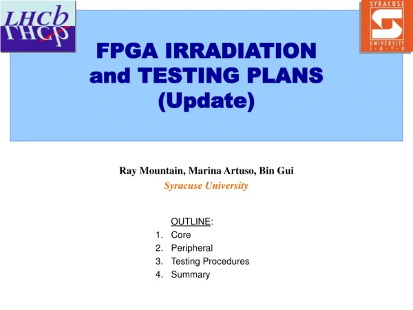
FPGA IRRADIATION and TESTING PLANS (Update). Ray Mountain, Marina Artuso, Bin Gui Syracuse University. OUTLINE : Core Peripheral Testing Procedures Summary. “DESIGN FLOW” of PROJECT. First stage: Concentrate on internal/core workings of A3PE1500 Understanding core behavior of FPGA

E N D
FPGA IRRADIATION and TESTING PLANS(Update) Ray Mountain, Marina Artuso, Bin Gui Syracuse University • OUTLINE: • Core • Peripheral • Testing Procedures • Summary
“DESIGN FLOW” of PROJECT • First stage: Concentrate on internal/core workings of A3PE1500 • Understanding core behavior of FPGA • Using VHDL to configure logic cells, clocks, shift registers, etc. • Understand structure and use of RAM-blocks/Flash-ROM • Understand configuration and procedure • Second stage: Concentrate on “peripheral” connections • LVDS I/O and external (off-board) connections • JTAG interface • LabVIEW interface and control • Third stage: Concentrate on testing procedure • Develop, test, and refine algorithms • Last stage: Irradiation Tests • Packaging FPGA for tests • Irradiate FPGA • Identify failure modes, mitigation schemes here R. Mountain, Syracuse University Irradiation Testing of LHCb Upgrade front-end FPGAs, 26 Oct 2009 -2-
CORE • Reminder: We have Actel A3PE1500 FPGA evaluation kit, with FlashPro3 programmer • As of now, we have gained some experience in VHDL with this device (Bin), programming, simulating, and some understanding of its operation, etc. • Have a candidate x-board in hand for external communication (though probably not fast enough, as is) X-Board A3PE Eval Board PC LVDS LabVIEW IP/USB JTAG FlashPro3 USB JTAG R. Mountain, Syracuse University Irradiation Testing of LHCb Upgrade front-end FPGAs, 26 Oct 2009 -3-
PERIPHERAL • LVDS LOOP to set up off-board communication • Configured I/O ports properly • Tested running data through LVDS ports • Used external clock through LVDS ports • Interfacing with x-board for LVDS, JTAG (in progress) • Will re-test all at faster speeds LVDS LOOP R. Mountain, Syracuse University Irradiation Testing of LHCb Upgrade front-end FPGAs, 26 Oct 2009 -4-
TESTING PROCEDURE • Outline of irradiation testing procedure: • Run SEU Test algorithm (almost continuously). Cycle through different clock frequencies, to 40 MHz • Intersperse memory checks: • dynamic registers (RAM-blocks), R/W cycle • static registers (Flash-ROM), R only from core, W with JTAG if needed • Periodically check configuration for corruption (i.e., verify configuration and programmability of device) • Periodically cycle power on FPGA • Plus: global issues (reset lines), and dedicated tests (PLLs), as requested in survey R. Mountain, Syracuse University Irradiation Testing of LHCb Upgrade front-end FPGAs, 26 Oct 2009 -5-
SEU TEST (1) • Enter data, clock through “all” logic cells, compare at output. Use bitstream, random or pattern. • Run for different clockings up to 40 MHz to check for frequency dependence • This has been implemented and tested (on board, lower speeds) (offboard) Clock/Data 512-bit Shift Register 512-bit Shift Register LVDS I/O …. Target area for beam 512-bit Shift Register 512-bit Shift Register (may be onboard) Comparator Counter 512-bit Shift Register 512-bit Shift Register 512-bit Shift Register (offboard) FPGA (~38 shift registers) R. Mountain, Syracuse University Irradiation Testing of LHCb Upgrade front-end FPGAs, 26 Oct 2009 -6-
SEU TEST (2) • MAP of CHIP USAGE: • Core used: 96.3% (of 38400 cells) in this simplest configuration. • This will be the max. Need more space for I/O functions. • Fill as much as possible to get a cross section measurement. Will try to constrain from using corners. RAM BLOCKS I/O PORTS LOGIC CELLS R. Mountain, Syracuse University Irradiation Testing of LHCb Upgrade front-end FPGAs, 26 Oct 2009 -7-
MEMORY TESTS • Working on this part now… • Plan to include triple-voting checks • Store same number in three separate registers, read each one • Store number in a register, read three separate times • If SEE, should be the same rates • CAL: Need to clock RAM R/W up to 160 MHz ? R. Mountain, Syracuse University Irradiation Testing of LHCb Upgrade front-end FPGAs, 26 Oct 2009 -8-
CONFIGURATION TEST (1) • A3PE1500 is a Flash-based FPGA. • Has Flash-Switches as memory elements for core configuration, embedded in logic cells (~dozen per cell). • These are the configuration elements. The configuration is stored in switches, not in the Flash-ROM or RAM-blocks. • Cannot directly read back configuration file per se for verification (according to Actel engineer), using either Libero software or bare JTAG protocol. • JTAG signals talk to a state machine in A3PE which compares given configuration with stored configuration and returns verification pass/fail. • Since it is FSM, it is not simple. Also it is subject to rad damage effects (SEU etc.). So, if corrupted, cannot configure the FPGA. This may be the mechanism seen previously producing programming failures. Still looking into this… R. Mountain, Syracuse University Irradiation Testing of LHCb Upgrade front-end FPGAs, 26 Oct 2009 -9-
CONFIGURATION TEST (2) • Plan now is to verify running configuration periodically during irradiation. • Alternately, would like to program FPGA with more complicated configuration. • Soliciting a “real” configuration file, with real operations and use of registers, etc. Does not really have to function. Can someone provide us with one for this purpose? R. Mountain, Syracuse University Irradiation Testing of LHCb Upgrade front-end FPGAs, 26 Oct 2009 -10-
SUMMARY • Progressing on “Design Flow” • Have basic programming and chip operation in hand • Concentrating right now on off-board communications and memory checks • Questions: • Does this test all the aspects that people are interested in? • Would like ‘real’ configuration file as part of this, eventually • Please comment, or send me email • Schedule: • Plan is to do irradiation this year. Have not fixed the schedule yet, since we will need to progress further first. • If were to slip to early next year, is this a specific problem for anyone? R. Mountain, Syracuse University Irradiation Testing of LHCb Upgrade front-end FPGAs, 26 Oct 2009 -11-