Download
1 / 1
10 likes | 120 Views
In-situ Detection of the High Pressure Metallic Phase In Silicon. John A. Patten (WMU, Kalamazoo, MI 49008 ) Lei Dong, Jimmie A. Miller (UNCCharlotte, NC 28223) 2005 NSF DMII Grantees Conference, Scottsdale, Arizona.

E N D
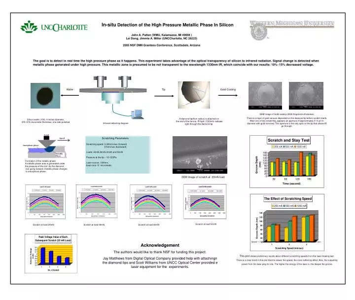
In-situDetection of the High Pressure Metallic Phase In Silicon John A. Patten (WMU, Kalamazoo, MI 49008 ) Lei Dong, Jimmie A. Miller (UNCCharlotte, NC 28223) 2005 NSF DMII Grantees Conference, Scottsdale, Arizona The goal is to detect in real time the high pressure phase as it happens. This experiment takes advantage of the optical transparency of silicon to infrared radiation. Signal change is detected when metallic phase generated under high pressure. This metallic zone is presumed to be not transparent to the wavelength 1330nm IR, which coincide with our results: 10%~15% decreased voltage. Wafer Tip Gold Coating Si Wafer Detector V SEM Image of Gold coating (2000 Angstroms thickness) There is a layer of gold vacuum deposited on the diamond tip before scratch starts. After one or two scratching, appears an aperture of approximately 3~4 um in diameter with gold removed. This aperture is the only spot on the tip that allows IR go through. A diamond tip(5um radius) is attached on the end of the ferrule. IR light (1330nm) radiates right through the diamond tip. Silicon wafer (100), 4 inches diameter, 475~575 micrometer thickness, one side polished Infrared detecting diagram Scratching Parameters Scratching speed: 0.305mm/sec (forward) 2.5mm/sec (backward) Loads: 20mN,30mN,40mN and 50mN Pressure at the tip: ~10-12GPa Laser source: 1330nm, beam size 10 micrometer, Formation of the metallic phase A metallic phase area is generated under the pressure of the tool. As the diamond tool going forward, metallic phase changes to amorphous phase. SEM Image of scratch at 20mN load Scratch at load 50mN Scratch at load 20mN Scratch at load 30mN Scratch at load 40mN Speed 1: 0.305mm/sec Speed 2: 0.002mm/sec Speed 3: 0.0002mm/sec Acknowledgement The authors would like to thank NSF for funding this project. Jay Matthews from Digital Optical Company provided help with attachingn the diamond tips and Scott Williams from UNCC Optical Center provided e laser equipment for the experiments. This plot shows preliminary results about different scratching speeds from the laser-heating test. There is a clear trend in this plot that the slower the speed, the more softening effect. Also, the outputting power from the laser play its role. The higher the energy of the laser is, the deeper the groove.