
Ultra Fast Analog Memories for Fast Photo-Detector Readout
This article discusses the use of ultra-fast analog memories for high-precision time measurement and waveform recording in photo-detector readout applications. It compares the performance and cost of different measurement chains and introduces a new sampling matrix solution. The article also presents the features and performance of the USB WaveCatcher board for autonomous testing and waveform analysis.

Ultra Fast Analog Memories for Fast Photo-Detector Readout
E N D
Presentation Transcript
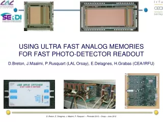
Using ultra fastanalogmemoriesfor fast photo-detector readoutD.Breton, J.Maalmi, P.Rusquart (LAL Orsay), E.Delagnes, H.Grabas (CEA/IRFU)
Introduction Photo-detectors are implied in all kinds of applications. Associated electronics can be used either for their characterization (test benches) or for their readout (experiments). For test benches: Ultimate performance of the electronics is requested If the number of channels is small (≤4), then high-end oscilloscopes can be used, but they are expensive. Dedicated hardware/software can also be very useful and effective If the number of channels increases, and if one wants to study all of them in parallel, difficulties occur. For physics experiments: Usually, dedicated ASICs are used They shape the signal and measure Amplitude, Charge and/or Time But, what happens if: Time measurement precision has to be (much) better than 30ps rms ? One wants to measure A, Q and/or T, but also see the waveforms on demand ?
The measurementchain Choice of measurementchainisdriven by the ratio performances/cost perchannel Control Testbench Oscilloscope Multipurpose test board Set of specialized boards Front End Board Acquisition Board Amplitude USB, Field Bus… USB, Field Bus… ADC Ethernet Preamp Amplitude/Charge/WaveForm QDC • FPGA: • Evt Buffer • Post-Processing: • digital filtering • - … ADC Processor Optical Links Gbits/s • FPGA: • Evt Buffer • PreProcessing: • FFT, CFD… • - … Charge FE Chip Preamp + CFD TDC TDC Time Photo-detector PCI/PCIx Time PC- Farm Trigger primitives Trigger, CLK, CMDs Analog Memory Clk & Ctrl System Trigger System Trigger
Circular analog memories: basic principles An analog memory can record waveforms at very high sampling rate (>>GS/s) After trigger, they are digitized at a much lower rate with an ADC (~20 MHz) • A write pulse is running along a folded delay line (DLL). • It drives the recording of signal into analog memory cells. • Sampling stops upon trigger. • Readout can target an area of interest, which can • be only a subset of the whole channel • Dead time due to readout has to remain as small • as possible (<100ns / sample).
Our favourite solution: a Sampling Matrix • We started designing analog memories in 1992 with the first prototype of the Switched Capacitor Array (SCA) for the ATLAS LARG calorimeter. 80000 chips produced in 2002, now on duty on the LHC. • Since 2002, 3 new generations of fast samplers have been • designed (ARS, MATACQ, SAM): total of more than30000 chips in use. HAMAC 1998-2002 Sampling at 3.2GS/s MATACQ 2000-2003 Readout 12 bits 20 MHz ADC Patented in 2001 SAM 2005 SAMLONG 2010-2012
Analog memories vs ADCs Analog memories actually look like perfect candidates for high precision measurements at high scale: Like ADCs they catch the signal waveform TDC is built-in (position in the memory gives the time) Only the useful information is digitized (vs ADCs) => reduced dataflow and power Any type of digital processing can be used Main difficulty is less sampling frequency than signal bandwidth Their drawbacks: The limited recording depth The readout dead-time limiting the input rate But: Only a few samples/hit can be read => this may limit the dead time Simultaneous write/read operation is feasible, which may further reduce the dead time
The USB_WaveCatcher board (V6) The module The autonomous test bench
Possibility to add an individual DC offset on each signal Individual trigger discriminator on each channel External and internal trigger + numerous modes of triggering on coïncidence (11 possibilities including two pulses on the same channel) => useful for afterpulse studies Real time trigger counting independent of acquisition rate Embedded charge mode (integration starts on threshold or at a fixed location) => high rates (~ 7 kEvents/s) Embedded pulse generators for reflectometry applications Board Specific Features This oscilloscope-like software was developed by the team.
Board performances: examples Comparison oscilloscope/WaveCatcher
Time characterization with digital CFD method Source: randomly distributed set of two positive pulses Results are the same with negative pulses or distance between arches of a sine wave A1 V relative threshold : constant fraction of the peak! A2 k x A1 A3 k x A2 k x A3 t Δt ~ 0 USB Wave Catcher Constant Fraction Discriminator Agilent 81110/12/12
Summary of the WaveCatcher performances. • 2 DC-coupled 1024-deep channels with 50-Ohm active input impedance • ±1.25V dynamic Range, with full range 16-bit individual tunable offsets • 2 individual pulse generators for test and reflectometry applications. • On-board charge integration calculation. • Integrated raw trigger rate counters • Bandwidth~ 500MHz • Signal/noise ratio: 11.8 bits rms • (noise = 650 µV RMS) • Sampling Frequency: 400MS/s to 3.2GS/s • Max consumption on +5V: 0.5A • Absolutetime precision in a channel (typical): • without time calibration: ~20ps rms (3.2GS/s) • after time calibration ~10ps rms(3.2GS/s) • Relative time precision between channels: <5ps rms. • Triggersources: software, external, internal, threshold on signals, • 11 modes of trigger coincidence • Acquisition rate (full events) Up to ~1 kHzover 2 full channels • Acquisition rate (charge mode) Up to ~7 kHzover 2 channels SiPM multiple photon charge spectrum 1 5
Applications to photo-detectors: a few examples
MCP-PMT characterization at SLAC (J. Va’Vra) Goal was to compare different electronics for measuring the signal time difference between 2 MCPPMTs => NIM paper A 629 (2011) 123–132 Tektronix oscilloscope Using Ortec modules Using Waveform Digitizers σ~3.4ps WaveCatcher board Digital CFD method was used Summary of electronics comparison Without walk correction With walk correction
PM characterization at APC • Goal is to precisely characterize the Antares opto-modules in single photoelectron mode • 1,000,000 triggers per measurement step • 0.45% of triggers give a photoelectron (=> ~1.5% of statistical error) • There are 289 measurement steps spaced by 1cm (3 degrees of aperture on the optical module) starting from its center • Using the integrated charge mode, reading out the 289,000,000 events takes only 2h30. 1 5
To validate the principle, we decided to build a synchronous 16-channel acquisition system based on 8 two-channel WaveCatcher V5 boards Technical challenge: to keep the 10ps time precision at the crate level Increasing the number of channels … 4-channel prototype 16-channel crate New controller board Mean differential jitter is of about 12ps rms which corresponds to 8.5 ps rms of time precision per pulse
TOF at the SLAC cosmic ray telescope • TOF experimental setup on the CRT • Goal was to measure the time difference in cosmic muon detection between the two quartz bars in view of SuperBFTOF prototype More thanadequate for final physicsgoal of 50 pswith 5 to 10 photoelectrons μ Trigger Time resolution between 2 channels Acquisition software
MCPPMT test benchat LAL SL10 test setup BURLE 85012 MCPPMT on its scanning setup SL10 test results Towards 16-ch crate
Latestdevelopments 2011 2010 …
2012 • The 16/18-channel board • 1.6mm thick • 10 layers • 233 x 220 mm² • 3200 components • 25 power supplies (5 global, 20 local) • 4 4-channel blocks (can be used as mezzanines on other boards) • 2 channels dedicated to digital signals
2-channel front-end diagram BACKPLANE Ch0 + Low Threshold - + High Threshold - Ch1 + ½ Front End FPGA (TimeStamp,Q,A) Low Threshold Trigger in - FPGA Controller + High Threshold - Trigger out Run, read Event data Ch0 SAMLONG (1024 samplingcells) clk 12-bit ADC Ch1 USB x 8
FPGA Interface block Reg Reg Reg Reg LP-in Fifo Fifo Fifo Fifo RAM RAM RAM RAM LP-out 0 LP-out 1 LP-out N FPGA LP-in LP-out 0 LP-out 1 LP-out M A flexible architecture thanks to LP-BUS FT2232H or …. USB/Ethernet Interface Needed if not interfaced with a FT2232H… internal registers, Fifos, RAMs … Layer 1 Multi-layer protocolbased on encapsulation and decapsulation of the data field. Arbitrer Protocol is adapted to tree architectures: same firmware blocks at all layers + possibility for broadcast access LP-Bus N LP-Bus 0 LP-Bus 1 FPGA FPGA LP-in LP-in Layer 2 Arbitrer Arbitrer Arbitrer LP-out M LP-out M LP-out 0 LP-out 1 LP-out 0 LP-out 1 Event fragments are pushedtowards USB => thispermits a sparsifiedreadout => canbebased on the dual signal threshold
Present and futureboardfeatures (not exhaustive) Possibility to add anindividual DC offset on each signal 2 individualtrigger discriminatorson eachchannel External and internal trigger + numerous modes oftriggering on coïncidence Embedded charge mode (integrationstarts on threshold or at a fixed location) => high rates (~ 3.5 kEvents/s) 2 extra memorychannelsfor digital signals One pulse generatoron each input Externalclockinput for multi-board applications Embedded USB and Serial Lite/Fibre Channel/Conet interfaces Possibility to program the FPGAs via USB/Backplane/AlteraBlaster Possibility to chainchannels by groups of 2 Embeddeddigital CFD for time measurement Embeddedsignal amplitude extraction
Front-end block can be used as a mezzanine The latter has been mounted on a CAEN USB-drivendigitizermotherboard Almostfullyvalidated! Measurementsresults are equivalent to those of the WaveCatcher module: noise level : 0.72 mV, signal bandwidth ~ 500 MHz, time precision < 10ps rms
16-channel acquisition software Main panel: oscilloscope like Time measurement panel
Building large scalesystems Layout of the controllerboard 64-channelbackplane • To synchronise N boards a controllerboardisneeded + backplane for the interconnections • we are building a very compact 64-channelsystem: • willsoonbeused for the CORTO Cosmic Ray Telescopeat Orsay • we are also building a 320-channel system in 6U-crate (SuperNemoexperiment)
Continuing R&D: SAMPIC, the 5-ps TDC R • We started designing the SAMPIC ps TDC six months ago => This ASIC makes use of the new AMS 0.18 µm CMOS technology • First version will house 8 blocks of 64 analog memory cells • Sampling is performed between 2 and ~10 GS/s • Signal bandwidth is ~ 1 GHz • Digitization will be performed inside the chip with a parallel 10-bit Wilkinson ADC running at 2 GHz in each cell • The 2-GHz clock is not distributed to the cells but runs a unique gray counter • The cells house a fast comparator and a latch • Submission is targetted for July 2012 • First tests should take place in September • Works on analogsignals • Producestime and digitizedwaveform ! Critical path for time measurement One SAMPIC channel
Conclusion Photo-detectors are implied in all kinds of applications. Associated electronics can be used either for their characterization (test benches) or for their readout (experiments). For test benches: if the number of channels is small (≤4), then high-end oscilloscopes are commonly used. For small budgets, analog memory-based acquisition boards can do the job for cheap. If the number of channels increases, and if one wants to study all of them in parallel, analog memories are good candidates for a reasonable price For physics experiments: Dedicated A/Q/T ASICs are a natural option But if one wants to see the waveforms, or if time measurement precision has to be (much) better than 30psrms, analog memories seem to be the right answer R&D is going on: the multi-channel SAMPIC TDC will soon produce both 5-ps timing and signal waveforms …


