Download
1 / 2
20 likes | 130 Views
Introduce nanoscience to education at JSU through student research on novel Cu-W alloy films via AFM & STM, focusing on high temperature stability and mechanical strengths. Training students in nanostructured materials' processing and characterization for various applications.

E N D
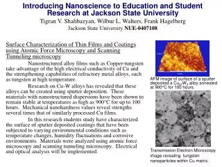
Introducing Nanoscience to Education and Student Research at Jackson State University Tigran V. Shahbazyan, Wilbur L. Walters, Frank Hagelberg Jackson State University NUE-0407108 Surface Characterization of Thin Films and Coatings using Atomic Force Microscopy and Scanning Tunneling microscopy Nanostructured alloy films such as Copper-tungsten take advantage of the high electrical conductivity of Cu and the strengthening capabilities of refractory metal alloys, such as tungsten at high temperature. Research on Cu-W alloys has revealed that these alloys can be created using sputter deposition. These materials with nanostructured dispersions have been shown to remain stable at temperatures as high as 900°C for up to 100 hours. Mechanical nanohardness values reveal strengths several times that of similarly processed Cu films. In this research students study have characterized the surface of sputter deposited coatings that have been subjected to varying environmental conditions such as temperature changes, humidity fluctuations and corrosive environments. Materials were analyzed using atomic force microscopy and scanning tunneling microscopy. Electrical and optical analysis will be implemented. AFM image of surface of a sputter deposited a Cu97W3 alloy annealed at 900°C for 100 hours. Transmission Electron Microscopy image revealing tungsten nanoparticles within Cu matrix.
Introducing Nanoscience to Education and Student Research at Jackson State University Tigran V. Shahbazyan, Wilbur L. Walters, Frank Hagelberg Jackson State University NUE-0407108 Undergraduate Education and Outreach In this program students are trained throughout the academic year and the summer in the technologies of processing and characterization of nanostructured materials that are used in microelectronics, aerospace, flexible displays etc. Training includes hands-on experience in sol-gel and polymer film processing, scanning tunneling microscopy, atomic force microscopy, optical spectrophotometry and electrical characterization systems. Currently 11 students from varying departments are involved in research and mentoring activities. These initiatives are fostered by: 1. Introductory Nanotechnology lecture and laboratory courses that focus on materials processing and characterization, 2. A Nanotechnology Seminar Series, and 3. Summer Internships and Co-ops in private industry, government laboratories and major academic research institutions.