Multiple - Cycle Hardwired Control
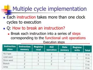
Multiple - Cycle Hardwired Control. Single-Cycle Computer Issues. Shortcoming of Single Cycle Design Complexity of instructions executable in a single cycle is limited Accessing both an instruction and data from a simple single memory impossible

Multiple - Cycle Hardwired Control
E N D
Presentation Transcript
Single-Cycle Computer Issues • Shortcoming of Single Cycle Design • Complexity of instructions executable in a single cycle is limited • Accessing both an instruction and data from a simple single memory impossible • A long worst case delay path limits clock frequency and the rate of performing instructions • Handling of Shortcomings • The first two shortcomings can be handled by the multiple-cycle computer discussed here • The third shortcoming is dealt with by using a technique called pipelining
Multiple-Cycle Computer • Converting the single-cycle computer into a multiple-cycle computer involves: • Modifications to the datapath/memory • Modification to the control unit • Design of a multiple-cycle hardwired control
Datapath Modifications • Use a single memory for both instructions and data • Not essential to the multiple-cycle design, but done to illustrate the concept • Requires new MUX M with control signal MM to select the instruction address from the PC or the data address • Requires path from Memory Data Out to the instruction path in the control unit
New Instruction Path Inst. & Data Address Mux Inst. & Data Memory
Datapath Modifications (continued) • To hold operands between cycles, need additional registers • Add 8 temporary storage registers to the Register File • Register File becomes 16 x 16 • Addresses to Register File increase from 3 to 4 bits • Register File addresses come from: • The instruction for the Storage Resource registers (0 to 7) • The control word for the Temporary Storage registers (8 to 15) • The control word specifies the source for Register File addresses • Add Register Address Logic to the Register File to select the register address sources • Three new control fields for register address source selection and temporary storage addressing: DX, AX, BX
Register Address Logic 16 x 16 Register File
Control Unit Modifications • Must hold instruction over the multiple cycles to draw on instruction information throughout instruction execution • Requires an Instruction Register (IR) to hold the instruction • Load control signal IL • Requires the addition of a "hold" operation to the PC since it only counts up to obtain a new instruction • New encoding for the PC operations uses 2 bits
Add "hold" operation Instruction Register IR
Sequential Control Design • In order to control microoperations over multiple cycles, a Sequential Control replaces the Instruction Decoder • Input: Opcode, Status Bits • Output: Control Word (Modified Datapath Control part) • Control State • Next State: Control Word (New Sequencing Control part) • Register to store the Control State • Combinational Logic to generate the Control Word (both sequencing and datapath control parts) • The Combinational Logic is quite complex so we assume that it is implemented by using a PLA
Control State Register Combinational Control Logic New/ Modified Control Word
Control Word 27 24 23 22 21 20 17 16 13 12 9 8 7 4 3 2 1 0 I M M R M M • Datapath part: fields DA, AA, and BA replaced by DX, AX, and BX, respectively, and field MM added • If the MSB of a field is 0, e.g., AX = 0XXX, then AA is 0 concatenated with 3 bits obtained from the SA field in the IR • If the MSB of a field is 1, e. g. AX = 1011, then AA = 1011 • Sequencing part: • IL controls the loading of the IR • PS controls the operations of the PC • NS gives the next state of the Control State register • NS is 4 bits, the length of the Control State register - 16 states are viewed as adequate for this design NS PS AX BX FS DX L B D W M W Sequencing Datapath
StateMachineDiagramsfor Sequential Control • An instruction requires two steps: • Instruction fetch– obtaining an instruction from memory • Instruction execution– the execution of a sequence of microoperations to perform instruction processing • Due to the use of the IR, these two steps require a minimum of two clock cycles
LoadRegisterIndirect (LRI) R[DR] <- M[M[R[SA]]]
0001101 0001110 Right Shift and Left Shift Multiple (SLM and SRM)