Download
1 / 21
210 likes | 386 Views
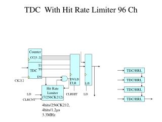
TDC With Hit Rate Limiter 96 Ch. Counter. CC[5..2]. TDC. T1 T0 DV. TDC/HRL. DVLD CLR. TDC/HRL. CK212. L/S. Hit Rate Limiter (7/256CK212). TDC/HRL. LD. CLRHIT. LD. TDC/HRL. CLRCNT. 4hits/256CK212, 4hits/1.2 m s 3.3MHz. TDC Data Concentration 96 Ch. 4hits/CH/1.2 m s

E N D
TDC With Hit Rate Limiter 96 Ch Counter CC[5..2] TDC T1 T0 DV TDC/HRL DVLD CLR TDC/HRL CK212 L/S Hit Rate Limiter (7/256CK212) TDC/HRL LD CLRHIT LD TDC/HRL CLRCNT 4hits/256CK212, 4hits/1.2ms 3.3MHz
TDC Data Concentration 96 Ch 4hits/CH/1.2ms 16hits/4CH/1.2ms 1hit: 16bits Buffer Length: (256/16)x1.2ms=19.2ms EV Window 2 x 1.2ms 128hits/16CH/EV 16 Ch Output Time: 128CK106=64RF=1.2ms 48 Ch Store Time:=3.6ms TDC/HRL SDRAM WR Time: 256RF<4.8ms TDC/HRL Zero Supp. L1 Buffer 1xM4K 16x256 TDC/HRL SDRAM 16x6M/spill 12MB/spill TDC/HRL TDC/HRL TDC/HRL Zero Supp. L1 Buffer 1xM4K 16x256 EV Buffer 2xM4K 16x256x2 TDC/HRL FPGA (DCC) TDC/HRL L1 Buffer 1xM4K 16x256 Truncating at EV Buffer 123+5 words/48CH/EV 48 Ch Send Out Time: 128x2RF=4.8ms L1 Buffer 1xM4K 16x256
Readout Timing 1.2us 0 1 2 3 4 5 6 7 8 9 a b c WR 0,1 0,1 0,1 6.6us RD G0 B=0 G0 B=1 G4 B=0 G4 B=1 G8 B=0 G8 B=1 G12 B=0 G12 B=1 G16 B=0 G16 B=1 G20 B=0 G20 B=1 G24 B=0 G24 B=1 G28 B=0 G28 B=1 G32 B=0 G32 B=1 G44 B=1 1.2us
17 16 15 14 13 12 11 10 9 8 7 6 5 4 3 2 1 0 Data Format 0 0 0 No Data 1 0 0 EHID[5..0] CNT[7..0] P EV Header 0 1 0 0 EV[13..0]=1, 2, .. 16K-1 P EV Header 1 CHGRP Header 1 0 1 0 TS[7..0] BD_CHGRP[4..0] P 1 1 CH[3..0] CC[10..2] T1 T0 P Hit Data 0 0 0 Ender 1 0 1 1 Reserved Header/Ender P
Data Block No Data EV Header 0 EV Header 1 No Data No Data CHGRP Header CHGRP=0 EV Header 0 EV Header 0 Hit Data EV Header 1 EV Header 1 Hit Data CHGRP Header CHGRP=0 CHGRP Header CHGRP=3 CHGRP Header CHGRP=1 Hit Data Hit Data CHGRP Header CHGRP=2 Hit Data CHGRP Header CHGRP=4 Hit Data CHGRP Header CHGRP=1 CHGRP Header CHGRP=5 CHGRP Header CHGRP=3 CHGRP Header CHGRP=2 Ender (=No Data) Hit Data Hit Data CHGRP Header CHGRP=4 Ender (=No Data) CHGRP Header CHGRP=5 Ender (=No Data)
TDC Description • The TDC FE card has three FPGA devices: two named MIPP_TDC and one named MIPP_DCC. Each MIPP_TDC digitizes 48 channels of inputs and sends data to MIPP_DCC which interfaces with a 16MB SDRAM and the daisy-chained interface to ship data back to the controller. A TDC_FE card supports 96 input channels. • Each channel in the MIPP_TDC has a hit limiter. The time is split into 1.2us (or 64RF, RF=1/53MHz) periods which are counted after the reset at the start of each spill. In each of the 1.2us, the number of hits in each channel is limited to 4 hits. • A channel group contains 4 channels. Every 4 cycles of CK106 (106MHz), hit data in each channel is written to the hold-shift register. The hold-shift register then shift data of the 4 channels, one in each CK106 cycle, to the zero suppression block. Therefore, the hit separation in each channel is 4 x 1/106MHz = 37.7 ns. • The zero-suppressed data from the 4-channel groups, i.e., only the valid hits are stored in the L1 pipeline buffers. A pipeline buffer is organized as 16 blocks of 16 words with 16-bit/word which uses a M4K RAM. Each hit is stored as a 16-bit word, each channel can have maximum 4 hits in 1.2us. Therefore, a 16 words block holds data of 4 channels in 1.2us. The entire L1 pipeline length is 16x1.2us = 19.3us. • Up to about 18us trigger latency are supported. For each trigger, data in 2 x 1.2us time window are readout, which corresponding to 2 16-word blocks in the L1 pipeline buffer. Data from 16 channels are grouped together, taking 1.2us to transfer from the L1 pipeline buffer to the EV buffer. Data of 48 channels are transferred in 3.6us. • Truncating happens while storing data into EV buffer if too many channels are hot. The data for an event stored in the EV buffer contains 2 headers and 3 enders, one at the end of each 16-channel group. The total number of hits allowed in 48 channels is 123. The truncated data block is not good for experiment data, however, it contains all necessary header and enders to avoid hanging up the remaining readout system. • Up to 256 16-bit words/event for 96 channels are stored in the 16MB SDRAM. A total of 32K events can be held in the SDRAM. • Daisy chained 8 TDC_FE cards are readout through a 26.5Mbit/s data link to the controller. The total time to readout 8 x 16 MB is about 48.3 sec.
TDC With Hit Rate Limiter Counter CC[5..2] TDC T1 T0 DV TDC/HRL DVLD CLR TDC/HRL CK212 L/S Hit Rate Limiter (7/256CK212) TDC/HRL LD CLRHIT LD TDC/HRL CLRCNT 7hits/256CK212, 7hits/1.2ms 5.8MHz
Reset Timing SCLR SCLRQ SCLRCC CC[9..2] 0 1 2 3 4 5 6 7 8 9 a b c d e f 10 ff 00 CLRHIT TCQ T=7 LD VTQ CH=0 CH=1 CH=2 CH=3 CLRCNT CK106 0 1 2 3 0 1 2 3 CC[4..3] 0 1 2 3 0 1 2 3 CCQ[4..3]=CH
Trigger Timing CC[9..2] FE FF 00 01 CLRCNT CC[9..3] 7F 0 1 2 3 CK106 TM1us 7E 7F 0 1 2 3 CCQ[9..3] WBK[2..0] BK1 BK1+1, BK1+4 Trig CC3Q[9..3] 7E 7F 0 1 2 3 TrigReq TM1us EVPRQ[7..3],[2..0] N,7 N+1,0 N+1,7 TMQQ[] (7E) (7F) (0) (1) (2) N,7 N+1,0 EVPR4Q[7..3],[2..0] EVPR5Q[7..3],[2..0] N,7 N+1,0 N+1,3 PUSHOK=!EVPR5Q[2] MGQ[] (7E) (7F) (0) (1) (7F)
TDC Data Concentration 7hits/CH/1.2ms 28hits/4CH/1.2ms 1hit: 16bits Buffer Length: (256/32)x1.2ms=9.6ms EV Window 2 x 1.2ms 448hits/32CH/EV Buffer Input Time: 448CK106=224RF =4.2ms TDC/HRL TDC/HRL TDC/HRL TDC/HRL Zero Supp. L1 Buffer 1xM4K 16x256 TDC/HRL TDC/HRL TDC/HRL EV Buffer 4xM4K 16x512x2 SDRAM 16x6M/spill 12MB/spill TDC/HRL Zero Supp. L1 Buffer 1xM4K 16x256 L1 Buffer 1xM4K 16x256 L1 Buffer 1xM4K 16x256 SDRAM WR Time: 448RF<9.6ms
L1 Buffer CCMLQ[12..10], CCQ[7..3] CCMLQ[12..10], CCQ[7..3] Event Window Zero Supp. L1 Buffer 1xM4K 16x256 VTQ0x VTQ1x CCQ[13..10] WA0x[4..0] WA1x[4..0] Zero Supp. L1 Buffer 1xM4K 16x256 0 0 CCP1Q[12..10], CCQ[7..3] CCP1Q[12..10], CCQ[7..3] CCQ[8]=1 CCQ[8]=0
Readout Timing 1.2us 0 1 2 3 4 5 6 2 3 4 5 6 7 WR 0 1 0 1 6.6us RD 2 1 3 0 4 7 G0 B=0 G4 B=0 G0 B=0 G4 B=0 G0 B=1 G4 B=1 G0 B=1 G4 B=1 5 6 G8 B=0 G12 B=0 G8 B=0 G12 B=0 G8 B=1 G12 B=1 G8 B=1 G12 B=1 G16 B=0 G20 B=0 G16 B=0 G20 B=0 G16 B=1 G20 B=1 G16 B=1 G20 B=1 G24 B=0 G28 B=0 G24 B=0 G28 B=0 G24 B=1 G28 B=1 G24 B=1 G28 B=1
Data Format 15 14 13 12 11 10 9 8 7 6 5 4 3 2 1 0 0 0 0 1 BD[2..0] CNT[8..0] 0 1 EV[13..0]=1, 2, .. 16K-1 D/H =1 CH[4..0] CC[9..2] T1 T0 256 x CK212 = 1.2ms 1024 x 1.18 ns 0 0 1 0 PR[1..0] TS[9..0] 0 0 1 1 Reserved Header/Trailer
TDC/HRL TDC/HRL TDC/HRL TDC/HRL L1 Buffer M4K 9x512 Zero Supp. Zero Suppression DV DV 1 0 Counter A==0 CH1 CH1 0 PUSH CH[3..0] CH0 CH0 0 CK212 CC5 CC5 X CC4 CC4 X CC3 CC3 X CC2 CC2 X T1 T1 X T0 T0 X Data Roll-over Marker 1/16CK212 1/4RF
L1 Buffer Contents 0 1 0 1 1 0 0 0 0 0 CH1 CH1 0 0 0 0 0 CH0 CH0 0 0 X CC5 X CC5 CC5 X X X CC4 X CC4 CC4 X X X CC3 X CC3 CC3 X X X CC2 X CC2 CC2 X X X T1 X T1 T1 X X X T0 X T0 T0 X X n+4 n+3 n+2 n+1 TS=n
Hold-Shift Timing SCLRQQ 0 1 2 3 4 5 6 7 8 9 a b c d e f 0 1 2 3 4 e f 0 CC[] SCLRTCQ LD53 CH[] 0 1 2 3 4 5 6 7 0 1 7 0 PUSH Counter CC[5..2] TDC DV T1 T0 DV Counter A==0 PUSH CH[3..0] DVLD CLR CK212 L/S Hit Rate Limiter (8/256CK212) SCLRTCQ LD13
POP Logic L1 Buffer M4K 9x512 EV Buffer 2xM4K 16x512 POP Logic Counter TS[11..0] DV CK212 TL TS-TP>TL TPL1-TP<TW etc. TW CH1 (A==0) &POPQ POP Counter CH0 INC L1 TP[11..4] PUSHEV CC3 DLSEL CK212 CC2 TL: 256 RF = 4.8ms TW: 16 x 4 RF = 1.2ms DLSEL: 64 CK212 for each group. CC1 CC0 S0. After Reset: No POP until TS-TP>TL S1. Before L1: Popping until TS-TP==TL S2. L1 Arrives: Stop popping, keep TPL1 S3. DLSEL: Resume popping PUSHEV if TPL1-TP<TW T1 T0
POP Logic L1 Buffer M4K 9x512 EV Buffer 2xM4K 16x512 POP Logic Counter TS[11..0] DV CK212 DL Token In TL CH1 TS-TP>TL DL Ctrl (A==0) &POPQ Counter CH0 INC TW TP[11..4] TPL1-TP<TW CC3 CK212 POP CC2 L1 DL Token Out TL: 256RF = 4.8ms TW: 16x4RF = 1.2ms CC1 CC0 S0. After Reset: No POP until TS-TP>TL S1. Before L1: Popping until TS-TP==TL S2. L1 Arrives: Stop popping, keep TPL1 S3. DL Token in: Popping until TPL1-TP==TW Output DL Token, go to S1. T1 T0
Hit Rate Limiter • For each incoming hit, the accumulator is added by: • 32 most of time • (-1) when >=224 (i.e., 7*32). • For each clock cycle with no hit, the accumulator counts down by: • 1 most of time • 0 if the accumulator is empty. • Long term dead-time-free hit rate: • < 1/33*212MHz = 6.4 MHz. • Instantaneous dead-time-free hit rate: • < 6hit in any 256+6 time window. • Absolute maximum number of hits in any 256 cycle (1.2ms): • 15 hits DVLD DV NE7 S NE0 0 0 +/- CK212