Download
1 / 12
130 likes | 180 Views
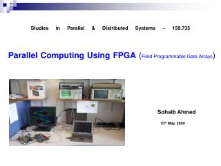
This introductory guide covers the basics of FPGAs, including CLB slice structure, LUT functionality, advantages of using FPGAs, FPGA design flow, and the Digilent Spartan-3 board. Learn how FPGAs offer configurable logic blocks, I/O blocks, block RAMs, and more, allowing for customizable hardware functionality without the need for extensive wiring. Discover how FPGAs streamline digital computing tasks and enable complex logic designs in an easily testable and debuggable manner. Explore the benefits of FPGAs over traditional circuit design methods using TTL chips.

E N D
Introduction toField Programmable Gate Arrays (FPGAs) COE 203 Digital Logic Laboratory Dr. Aiman El-Maleh College of Computer Sciences and Engineering King Fahd University of Petroleum and Minerals
Outline • What is an FPGA • CLB Slice Structure • LUT (Look-Up Table) Functionality • Advantges of using FPGAs • FPGA Design Flow • Digilent Spartan-3 Board • FPGA Device Part Marking
What is an FPGA?… • A filed programmable gate array (FPGA) is a reprogrammable silicon chip. • Using prebuilt logic blocks and programmable routing resources, you can configure these chips to implement custom hardware functionality without ever having to pick up a breadboard or soldering iron. • You develop digital computing tasks in software and compile them down to a configuration file or bitstream that contains information on how the components should be wired together.
Block RAMs Block RAMs … What is an FPGA ? Configurable Logic Blocks I/O Blocks Block RAMs
CLB Slice Structure • Each slice contains two sets of the following: • Four-input LUT • Any 4-input logic function, • or 16-bit x 1 sync RAM • or 16-bit shift register • Carry & Control • Fast arithmetic logic • Multiplier logic • Multiplexer logic • Storage element • Latch or flip-flop • Set and reset • True or inverted inputs • Sync. or async. control
LUT (Look-Up Table) Functionality • Look-Up tables are primary elements for logic implementation • Each LUT can implement any function of 4 inputs
CLB CLB CLB PSM PSM Programmable Switch Matrix CLB CLB CLB PSM PSM CLB CLB CLB Routing Resources
Advantages of using FPGAs • Creating intricate circuit designs from discrete parts, such as TTL chips, can be very tedious and error prone. • It can take a large number of chips to create a design of only moderate complexity. • It takes a lot of time to wire together a large number o f chips. Additionally, it can often be difficult to find misplaced wires when debugging a complex circuit. • Using FPGAs, it is possible to implement a complex logic design in a manner which is easy to test, debug and even change. • Using FPGAs, If the device does not function as it should, it is only necessary to debug the program as opposed to debugging the wiring of a circuit made from discrete chips.
Digilent Spartan-3 Board • 200K gate Xilinx Spartan-3 FPGA • 8 slide switches • 4 pushbuttons • 8 LEDs • 4-digit seven-segment display • Serial port • VGA port • PS/2 • And others ....
FPGA Device Part Marking We’re Using: Spartan 3 XC3S200-ft256