Download
1 / 24
240 likes | 260 Views
Analyzing radiation effects on detectors, focusing on charge collection efficiency, current transients, and defect generation. Investigating field redistribution and optimal design modifications. Evaluating Ramo's theorem in non-static conditions for signal amplification.

E N D
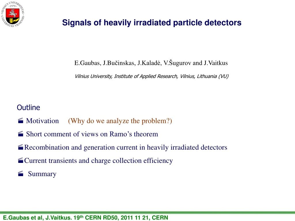
Signals of heavily irradiated particle detectors E.Gaubas, J.Bučinskas, J.Kaladė, V.Šugurov and J.Vaitkus Vilnius University, Institute of Applied Research, Vilnius, Lithuania (VU) • Outline • Motivation (Why do we analyze the problem?) • Short comment of views on Ramo’s theorem • Recombination and generation current in heavily irradiated detectors • Current transients and charge collection efficiency Summary
The main aspects: Many different centers are observed and they differently depend on the fluence but the capture time of carriers linearly decreases with increase of fluence. The radiation induced defects change the I(V) dependence of detector: • The reverse current increases a few orders of magnitude • I(V) becomes similar to the asymmetric resistor The Charge Collection Efficiency (CCE) decreases with the fluence, but: • It restores by an increase of bias • It was observed CCE more than 100 % in highly irradiated samples
Then it follows(if the structure becomes as photoresistor, and if the electrostatic approximation is valid): • The generation of deep levels in the midgap enhances the generation current in the structure, and it change an electric field distribution in it. • The radiation creates a main free carrier capture centre, and its efficiency linearly increase with the fluence, i.e., the capture probability depends on the distance between centers. • Therefore the CCE depends on the ratio of free carrier diffusion time to the capture center and its drift time through the base of detector. diffusion/ttransit diffusion = d2/4D, d – distance between the centers, D - diffusitivity
The questions: • Is any change of mechanism of the response on the excitation in a case of increase of generation current in the structure? • Does the structure become as a photoresistor? • What is the detector response time, i.e., RC? • Do the moving carriers induce the response in the circuit, or there is only the photoconductivity signal • What is an origin of CCE>100% in high fluence samples? • If it is caused by impact ionization, why it is absent in the lower irradiated samples?
The answers could show the ways to improve the properties of detector: • If the detector operates as the photoresistor, • then the increase of CCE depends on the ratio of lifetime/ttransit , • then better results will be in the higher bias devices and it could be recommended • to increase of lifetime but not more than the collection time. • If the detector is the relaxation type (the electrostatic approximation is not valid), and in any case, the understanding of conductivity mechanism (electric field distribution) and signal formation process is necessary to understand.
Motivation of the MORE GENERAL analysis • To predict signal changes and to foresee possible modifications of the detector design and voltage regimes • To evaluate the field redistribution effects • To evaluate the optimal thickness and doping parameters To evaluate processes of the signal amplification I.e., as a great role is given to the Ramo’s theorem in analysis of the signal formation, it is actual to look on it in more details, because Ramo’s model is an electrostatic approach that is correct if the processes are slow.
Si • Dielectric permittivity /0 =11.9 • 0 =8.85 10-14 F/cm • Conductivity – 10-2 – 10-4 -1cm-1 • = RC = 0/ As the conductivity of detector material is 10-2 – 10-4 -1 cm-1, therefore it appears a question: what influence on the Ramo approximation makes this non-static behaviour. i.e., electrostatic approach fits worse and worse if the compensation of semiconductor increases
A validity of the Ramo’s approximation • It was analyzed in many works, because a straight transfer the vacuum conditions to the semiconductor is not possible. • We concentrate on the results of: • I.V.Kotov, NIMA 539, 267-268 (2005) • L.A.Hamel, M.Julien. NIMA 597, 207-211 (2008) • and we performed some additional analysis starting from more general principles. • Our attempt to analyze the electrodynamic approach will be in a future because calculations prolonged more time than was proposed.
r Ramo’s theorem and it’s validity Ramo’s theorem based on energy balance using Green’s and Gauss’ theorems with specific boundary conditions The same technique was used by I.V.Kotov L.A.Hamel, M.Julien approach - local field conception, (but the boundary conditions different from p-i-n diode) In this work: a) the solution of the Poison equation (JB) b) the boundary conditions different from p-i-n diode included (EG) c) space charge effects neglected (JK) • Ramo’s boundary conditions • is the potential of the electrostatic field, • in the region between conductors 2 = 0 (R1) • eis the potential of the tiny sphere and on the conductors • j =0 (R2) • Electron removed, conductor j=A raised to unit potential • j=A’=1 V, (R3) • and the other conductors grounded. Call the potential of the field in this case', so that 2’ = 0 (R4) • QA A’= - e e - Ramo classical equation. actually, balance of electrostatic energy with A’=1V The linear inter-electrode media without any space charge excepted elementary one q=e For capacitor: CeA/t=0, for diode: CeA/t0
Ramo’s theorem and it’s validity Interpretation of Hamel-Julien based on analysis of electrostatic energy balance The charge Q induced in an electrode just behind the movement (single-dimensional, two-electrode approach) region z=H (i.e. brought from the external circuit into the electrode) by the movement of a single carrier of charge q over a distance z is given by Q =q z/H= q U/U (1) This is equivalent to calculating the charge Qj induced in electrode j when the test charge is moved from the ground, where el = 0, to the final position r. In this case, Eq.(1) is replaced by j=1NQjUj=-qel(r)= qjNj(r) with el(r)=jNj(r) (2) If all Uj are 0 except one j=A(r) which is at 1V, then the potential is simply el(r)= j=A(r), which is then equivalent to electrode j’s weighting potential jw(r). This is Ramo’s classical result, albeit jw(r) now includes the induced surface (Q Uj) and space charge (q el(r)) potentials explicitly: Qj = -q el(r)/Uj=qjw(r), i.e. jw(r)= el(r)/Uj (3) The second way (Hamel-Julien approach) to use Eq.(2) is to take the derivative with respect to Uj while keeping the other potentials constant at their operating biases: Qj| Ubias=-q[el(r)/Uj]|Ubias =qjwHJ(r), with jwHJ(r)= [el(r)/Uj]|Ubias (4) In a linear media, Eqs. (3) and (4) are fully equivalent. The classical result Eq.(3) does not hold true for non-linear (e.g. diode) media (L=H):
Ramo’s theorem and it’s validity (JB) 20 Electro-static approach - direct Poison equation solution Invalid Ramo’s boundary conditions R1, R3 If the solutions will be used in the HJ approximation, the dependence on “z” is obtained. Ramo’s case (moving charge potential causes capacitance change) QA= - ee/ A’ = CeAe Hamel-Julien Hamel-Julien approach, when e is not proportional to A’ like in non-linear media
Ramo’s theorem and it’s validity According P.Blood, J.W. Orton. Extended depletion approximation (non analytical case, numeric evaluation). Invalid R1, R3, R4 Diode: Wd in approach more rigorous than depletion approximation (Wa) Wa(20U/qND)1/2 simple depletion approximation ND~1012 cm-3 H=d= 300 m
Ramo’s theorem and it’s validity qe=8*10-13 C/cm2 20 Approach (EG) of diode (at depletion approximation) with induced surface charge qe at z0 HJ and EG Additional term related to the moving charge appears Ramo Hamel-Julien zx0
Ramo’s theorem and it’s validity Diode (at depletion approximation) with induced inhomogeneously distributed charge Ramo’s invalid 20 - invalid R1 Actually, Hamel-Julien approach of local Ramo’s field helps only in evaluation of instant weighing field. Due to Wqd(t), this field (=1/Wqd(t)) varies with time during charge drift (tdr) : q(t)=eNDeff(t) Wqd(q,t)- eNDeff(t)z(t)/[1-e-(tdr +t0)/M] t0- duration of excess carrier (nex –pex) pairs separation Hamel-Julien Approach of diode (at depletion approximation) with induced inhomogeneously distributed charge domain qe= qe0(z0)exp[-(z-z0)] 2’0 invalid R4, 2’=- qe(z0)exp[-(z-z0)]|0, -charge domain width <Eqe>=enex0-1[1- exp(-)]/20; qe0=enex0-1 EG approximation Complementarily, broadening of the induced excess carrier domain (t)= 0+(E)t leads to an increase of the transient current within ulterior phase of the induced current pulse
Ramo’s theorem and it’s validity including traps Using simple Ramo’s relation but including trapping as qe(t) QA= - qe(t) e/A’ with qe(t)=qe0exp (-t/capt) Generally, Ramo’s approximation is doubtfull IR=QA/t= qe(t){(1/A’)[q/z]}(z/t) -(qe(t)/capt)(q/ A’)= = qe(t)Ewjv- (qe(t)/capt)(q/ A’)=qe(t)[Ewjv-(1/capt)(q/ A’ )] • For capt (A’/ e)>> drift 1/Ewjv, and scale of tdrift, qe(t)=qe0= const, • and at q/ A’1, then, current leads to • IR(t)= qe0Ewjv , during t<drift , and • IR(t)=0 , for tdrift , charge drift is recorded Ramo’s approximation is valid CCE=(1/qMIP)[IR(t)dt] 2) For capt (A’/ e)<< driftqe(t)=qe0exp(-t/capt) current follows recombination decay IR(t)= (qe0/capt)exp (-t/capt) for all the time (t) scale; then, charge drift cannot be resolved Ramo’s approximation is invalid (A’/ e) should be known In the linear casedrift=d2/U, - then and only then Ramo’s relations are valid. Therefore, to keep condition (1), it is necessary to increase U and to decrease d.
Approach of diode (at depletion approximation) with induced surface charge domain q and including generation {NDeff(t)=ND(NT –nT(t)}, induced charge capture qe(t)=qe0exp (-t/C) currents and domain drift vq=dz0/dt Induced current within diode EG approximation: Displacement current: pseudo-Ramo’s component Conductivity (within transitional layer at Wq boundary) current due to q capture within SCR Conductivity (within transitional layer at Wq boundary) current due to thermal emission from fast (shallow) filled traps
If the electrostatic approximation is valid: • Analysis shows that if the generated charge is very small then the signal is related with to the generation and capture components. • If the induced charge is bigger then the signal start to depend on the redistribution of charge inside the detector (and the photoelectrical gain has to be observed).
Additional experimental findings: • Generation current evaluated from I(V) and it destroys the C(V) (and DLTS) analyzis. • Capacitance of diode reaches the geometrical capacitance value at fluence ~ 1015 cm-2 and more • The lifetime decrease corresponds to the generation current increase.
Carrier generation/emission lifetimes in Si detectors (for Mrad>>n0) Nearly linear reduction of generation lifetime with enhancement of fluence is similar to that of of recombination lifetime characteristic Qualitative emission lifetime dependence on fluence can be estimated from I-V C-V vs. fluence I-V vs. fluence after E.Gaubas et al JAP, 110 (2011) 033719 after E.Gaubas et al JAP, 110 (2011) 033719
Barrier capacitance of Si pad-detectors as a function of reactor neutrons fluence after E.Gaubas et al JAP, 110 (2011) 033719
If the semiconductor works as photoresistor: Photo-conductivity gain (PCG) The process will repeat until electron will recombine, or the hole will be extracted to the contact. PCG=tdr,h/tdr,e CCE>1 if tdr,e<tdr,h<Rec CCE0 for Rec<tdr
Summary 1 • Ramo’s theorem with some corrections is “partly” working but the electrodynamic approach is necessary to solve for the investigation the processes in the high resistivity Si. Space charge, and trapping, leads to more complicated description of current transients. • The high resistivity material based pin diodes become bad capacitors (with long relaxation – small operational frequency) under high irradiation fluences. (Only carriers emitted from shallow levels are able to be in equilibrium with band, which determine operational characteristics of detector. Deep levels actually do not govern the conductivity type).
Summary 2 For high density of traps and small carrier density, S-R-H recombination statistics is invalid, and relaxation is determined co-existence of many different centres which contribution is controlled by the hole capture rate (A.Rose model). Heavily irradiated diode behaves like a slow capacitor or un-stable resistor. There photo-electrical gain effect is probable. Also, the impact ionization avalanche causedgain is possible within electrode edge region when a virtual photo-electrode is formed by high density of photo-generated excess carriers.