Download

1 / 13
130 likes | 147 Views
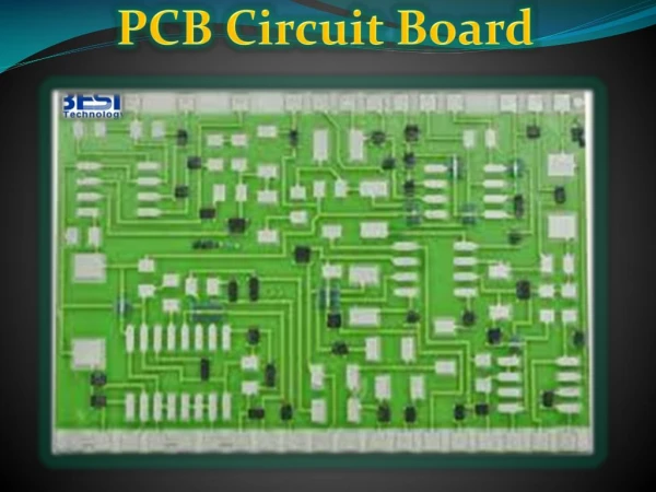
A multilayer PCB board is made from three or more conductive copper foils. These are glued and laminated together with layers of insulation between them. We useu00a0VIASu00a0to achieve electrical connections between the layers. This allows us to make complex PCBs of various sizes.<br>The electronic products are becoming sophisticated with time and we need advanced PCBs. Conventional PCBs had problems like crosstalk, noise, and stray capacitance. So, we had to follow some design constraints. However, these design constraints didnu2019t allow for the satisfactory performance of single-layer PCBs. Therefore, manufacturers came up with a multilayer PCB board.<br>

E N D
The Limitation of Multilayer PCB Board is Possible to be Solved A multilayer PCB board is made from three or more conductive copper foils. These are glued and laminated together with layers of insulation between them. We use VIAS to achieve electrical connections between the layers. This allows us to make complex PCBs of various sizes. The electronic products are becoming sophisticated with time and we need advanced PCBs. Conventional PCBs had problems like crosstalk, noise, and stray capacitance. So, we had to follow some design constraints. However, these design constraints didn’t allow for the satisfactory performance of single-layer PCBs. Therefore, manufacturers came up with a multilayer PCB board. MOKO TECHNOLOGY https://www.mokotechnology.com/
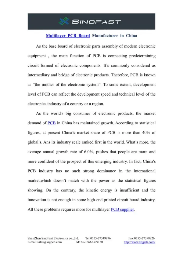
Multilayer PCB boards are gaining popularity in modern electronics. They are available in different sizes so we can use them for numerous applications. Multilayer PCB boards can have 3-50 layers. However, layers are mostly used in even numbers because an odd number of layers can lead to circuit warping. Common applications need no more than 12 layers of these PCBs however some special applications can involve up to 100 layers. However, this is very rare because it reduces their cost-effectiveness. 1 3 https://www.mokotechnology.com/ 4
Multilayer PCB boards are better than their alternatives When we compare multilayer PCB boards to the single layer or double layer PCBs, then the benefits of multilayer PCB boards seem more prominent. Here, we will take a look at some of them. Higher Assembly Density Single layer PCBs have limited density because of their surface area. However, we can multiply the density of multilayer PCB boards through layering. Therefore, we can increase their functionality, speed, and capacity and reduce their size. https://www.mokotechnology.com/
Multilayer PCB boards are better than their Smaller Size Multilayer PCB boards have a smaller size in comparison to the single layer PCBs. We can increase the surface area of single layer PCBs only by increasing their size. However, we can increase the surface area of multilayer PCB boards by adding more layers. So, we can decrease their overall size. This allows us to use multilayer PCB boards even in very small electronic devices. Lighter Weight We can seamlessly integrate a large number of components in multilayer PCB boards. So, we need a smaller number of connectors. Therefore, multilayer PCB boards are lightweight and are ideal for complex electronic applications. Multilayer PCB boards have the same functionality as that of a single-layer PCB. However, they require fewer connections and have reduced weight. This is empirical for smaller devices where we are concerned with the overall weight. https://www.mokotechnology.com/
Multilayer PCB boards are better than their Functionality Enhancement Multilayer PCB boards are more capable than the single layer PCBs. They have controlled impedance, greater design quality, and improved EMI shielding. So, we can accomplish more with them as compared to single layer PCBs. https://www.mokotechnology.com/
Multilayer PCB boards are better than their Multilayer PCB boards still exist some limitation Despite their advantages, multilayer PCB boards have some limitations. Therefore, we should also take a look at them. Higher Cost Multilayer PCB boards manufacturing is more expensive as compared to double layer and single layer PCBs. Multilayer PCB board design is difficult so we need more time to work out any possible problems. They have a complex manufacturing process so there are high labor costs. Additionally, the equipment we use for multilayer PCB boards fabrication is a little expensive. https://www.mokotechnology.com/
Multilayer PCB boards are better than their Complicated Production Multilayer PCB boards are difficult to manufacture and they require sophisticated manufacturing techniques. So, a multilayer PCB board can become useless even if there is a small flaw in the designing or manufacturing process. Need for Highly Skilled Individuals Multilayer PCB boards require extensive designing before we can manufacture them. If we lack experience then it can be very difficult. Interconnection is required between different layers of a multilayer board. However, we have to avoid impedance issues and crosstalk. Therefore, we need to be careful because a single flaw in the design can lead to a non-functioning PCB. https://www.mokotechnology.com/
Multilayer PCB boards are better than their Production Time There are more manufacturing steps involved as the complexity increases. This affects the turnover rate of multilayer PCB boards. Every multilayer PCB board needs a considerable amount of time to manufacture. This leads to longer wait times between when an order is placed and when you deliver the product. https://www.mokotechnology.com/
Tips for Designing Multilayer PCB boards Designing an efficient multilayer PCB board requires a lot of focus and care. So, here are some tips which can help you with the designing process. Board size If you set your board size first then it will give you a constraint for determining other elements of your multilayer PCB boards. The optimal board size depends on the size and number of components. It also depends on the location where you will mount your board, tolerance for spacing, drill holes, and clearances. Layer design You can use PIN density for finding the number of layers you will need for your board. For layer design, you should consider impedance requirements, especially if you are using controlled or fixed impedances. https://www.mokotechnology.com/
Tips for Designing Multilayer PCB boards VIAS selection The VIAS you choose for your board will affect the complexity of manufacturing. So, this will affect the quality of your multilayer PCB boards. Material selection You should select the material for manufacturing your board by using a layer by layer approach. However, you must ensure that the material allows for good signal integrity and ground plane distribution. Optimize the manufacturing process Your design decisions will affect the performance of your multilayer PCB board. You should carefully choose clearances, solder masking, drill hole sizes, and trace parameters. All of these significantly influence the manufacturing process. https://www.mokotechnology.com/
Thickness Standard for Multilayer PCB board The typical thickness of PCBs was 1.57 mm or 0.063 inches in the past. This was standardized because of the substrates of plywood sheets. However, when we started developing multilayer PCB boards then we had to follow the thickness of connectors between layers. So, the required thickness became variable. However, a general standard is thickness from 0.008 to 0.240 inches. You can choose the PCB thickness depending on your needs and applications. https://www.mokotechnology.com/
Thickness Standard for Multilayer PCB board https://www.mokotechnology.com/
MOKO Technology is a renowned name when it comes to manufacturing PCBs. We specialize in all kinds of PCBs including multilayer ones. We have the capability for mass production and we can incorporate any number of layers in our boards. If you are looking for a reliable supplier for custom made multilayer PCB boards service, then you are in the right place! Feel free to contact us if you want a quote or have any queries. MOKO TECHNOLOGY