Download
1 / 50
500 likes | 703 Views
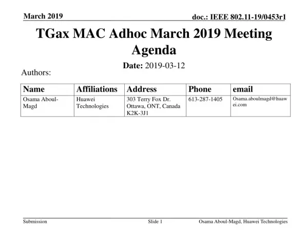
Subjects: ELECTRONICS/ENGLISH Teachers: Miria Bovino and Roberto Versari. ISTITUTO TECNICO INDUSTRIALE STATALE. GUGLIELMO MARCONI - Forlì. School Year 2009/2010. C.L.I.L. MODULE: ANALYSIS AND DESIGN OF FIRST ORDER RC FILTERS. Class: 4AEL. Outline of the CLIL module.

E N D
Subjects: ELECTRONICS/ENGLISH Teachers: Miria Bovino and Roberto Versari ISTITUTO TECNICO INDUSTRIALE STATALE GUGLIELMO MARCONI - Forlì School Year 2009/2010 C.L.I.L. MODULE:ANALYSIS AND DESIGN OF FIRST ORDER RC FILTERS Class: 4AEL
Outline of the CLIL module Lesson 1: RC low pass filter schematic and transfer function (with C.A.D. example) Lesson 2: frequency response graphical representation (with excel example) Lesson 3: Analysis of the CR high-pass filter (with excel + C.A.D. example) Lesson 4: An introduction to active filters and circuit simulations (with C.A.D. example) Istituto Tecnico Industriale Statale “G. Marconi” - Forlì
Lesson 1 Targets: Lesson 1: RC low pass filter schematic and transfer function (2h) Istituto Tecnico Industriale Statale “G. Marconi” - Forlì • Learn how to draw the schematic of an RC low-pass filter. • Learn how to calculate its transfer function G(jw) • Learn the filter constant time () definition • Learn how to calculate the RC low-pass filter output for any sinusoidal input. • Learn how to realize an RC low pass filter with a C.A.D. tool
The first order passive RC low pass filter is made of only two components: RC low pass filter schematic Istituto Tecnico Industriale Statale “G. Marconi” - Forlì R VO(jw) VI(jw) C output sinusoidal voltage stimulus or input sinusoidal voltage VI and VO can be represented by the corresponding vector quantities: VI=VIej, VO= VOej I O
Transfer function calculation (1/2) The RC low pass filter can be easily seen as a simple impedance divider with Z1=R and Z2=1/jwC Istituto Tecnico Industriale Statale “G. Marconi” - Forlì Z1=R VI(jw) Z2=1/jwC VO(jw) The impedance divider formula provides: VO/VI=Z2/(Z1+Z2). VO/VI is the transfer function G(jw) of the RC filter. Hence it is: G(jw)=Z2/(Z1+Z2)
Transfer function calculation (2/2) Let’s substitute Z1=R and Z2=1/jwC in G(jw) expression Istituto Tecnico Industriale Statale “G. Marconi” - Forlì . RC= [s] is defined as the time constant of the low-pass filter. Hence:
Output calculation (1/2) G(jw) is a complex number with: Istituto Tecnico Industriale Statale “G. Marconi” - Forlì • Amplitude: • Phase: . VO=G(jw) VI can be written using complex numbers properties: • VO Amplitude: • VO Phase: G(jw) depends only on and f (input signal frequency)
Output calculation (2/2) Istituto Tecnico Industriale Statale “G. Marconi” - Forlì RC low-pass filter . VI, I, f =RC VO, O, f G(jw) G(jw) sinusoidal input sinusoidal output 1) VI, I and f are given 2) the filter schematic is known is calculated. 3) f and are known G(jw) and G(jw) are calculated . 4) VO =|G(jw)| VI is calculated 5) O = G(jw) + I is calculated
Output calculation example Istituto Tecnico Industriale Statale “G. Marconi” - Forlì Exercise: calculate the output VO of the circuit corresponding to the given sinusoidal input VI 1) VI=1V, I=00, f=10KHz remember: 2) =RC=320*50nF=16s 3) |G(10KHz)|=1/ 1+(2**10KHz*16s)2 =0,7 G(10KHz)=-artg(2**10KHz*16s)=-450 The output voltage is attenuated of a factor of 0,7 and delayed of 45 degrees when f=10KHz. 4) VO=0,7*1V=0,7V 5) O=-450+00 =-450
LTspiceIV CAD tool Istituto Tecnico Industriale Statale “G. Marconi” - Forlì Download free from: http://www.linear.com/designtools/software • CAD tools: schematic implementation and real time simulation needed to decrease electronic circuit time to market. • English language prerequisite for most CAD tools.
Lesson 2 Targets: Lesson 2: RC low pass filter frequency response graphical representation(2h) Istituto Tecnico Industriale Statale “G. Marconi” - Forlì • Learn the graphical method to calculate any filter output. • Learn the low-pass filter cutoff frequency (fC) definition, its bandwidth (Bw) and the relationship between fC and . • Learn how to read and draw first-order low pass filters amplitude diagrams in logarithmic scale. • Learn how to design an RC low-pass filter for a given bandwidth and/or fC. • Learn how to draw the amplitude and phase diagrams of first-order RC low-pass filters with MS-excel.
The graphical approach to the calculation of filter output Istituto Tecnico Industriale Statale “G. Marconi” - Forlì • Lesson 1 result: the filter output voltage can be derived by the knowledge of the input voltage and the analitycal calculation of the filter transfer function G(jw) – both amplitude and phase. • Disadvantages of the analitycal approach: - two calculations (amplitude and phase) for each input frequency. - G(jw) analitycal expression depends on filter topology. • New graphical approach: two plots, namely |G(jw)| vs. f and G(jw) vs. f are associated to each filter. The calculation of the output voltage does not need G(jw) value calculation because the values of amplitude and phase of G(jw) at the given frequency can be simply read from the two given plots of the filter.
Amplitude and Phase diagrams |G(jw)| vs. f is the filter amplitude diagram* Istituto Tecnico Industriale Statale “G. Marconi” - Forlì G(jw) vs. f is the filter phase diagram* . Examples of amplitude and phase diagrams of an RC low pass filter with R=1K and C=1F. *=remember that:
Output amplitude calculation with graphical method (1/2) Istituto Tecnico Industriale Statale “G. Marconi” - Forlì RC low-pass filter amplitude diagram VI, f VO, f sinusoidal input sinusoidal output 1) VI, I and f are given 2) the filter amplitude diagram value at the frequency f can be read from the plot. . 3) VO =|G(jw)| VI is easily calculated, since |G(jw)| is the value read from the plot in step 2).
Output amplitude calculation with graphical method (2/2) Istituto Tecnico Industriale Statale “G. Marconi” - Forlì • Case 1): VI=1,5V I=00 f=100Hz From the filter amplitude diagram at f=100Hz we read |G(jw)| =0,8. Hence the output voltage amplitude at f=100Hz is VO=0,8*1,5V=1,2V • Case 2): VI=1,5V I=00 f=1KHz From the filter amplitude diagram at f=1KHz we read |G(jw)| =0,18. Hence the output voltage amplitude at f=1KHz is VO=0,18*1,5V=0,27V
Output phase calculation with graphical method (1/2) Istituto Tecnico Industriale Statale “G. Marconi” - Forlì RC low-pass filter phase diagram I, f O, f sinusoidal input sinusoidal output 1) VI, I and f are given 2) the filter phase diagram value at the frequency f can be read from the plot. 3) O = G(jw)+I is easily calculated, since G(jw) is the value read from the plot in step 2).
Output phase calculation with graphical method (2/2) Istituto Tecnico Industriale Statale “G. Marconi” - Forlì • Case 1): VI=1,5V I=00 f=100Hz From the filter phase diagram at f=100Hz we read G(jw)=-350. Hence the output voltage phase at f=100Hz is O=-350+0=-350 • Case 2): VI=1,5V I=00 f=1KHz From the filter phase diagram at f=1KHz we read G(jw)=-810. Hence the output voltage phase at f=1KHz is O=-810+0=-810 Graphical method advantages: - no need to calculate amplitude and phase: they are simply read from the plots. - it is a general approach valid for all kind of filters: it is only needed the knowledge of the amplitude and phase plots.
Amplitude diagram analysis Istituto Tecnico Industriale Statale “G. Marconi” - Forlì fC=160Hz stop band pass band B frequency scale is logarithmic 1) The cutoff frequencyfC is defined as the frequency value at which |G(jw)|=0,7 In fact, all input signals with f< fC “pass”, i.e. we can find them at the filter output without significant attenuation. On the contrary, all input signals with f> fC are “cut”, i.e. the filter output has an amplitude significantly lower than the input. 2) The filter band B is defined as the range of input frequencies for which the filter attenuation is 0,7. In practice B=[0, fC]. The bandwidth is the width of B=fC-0=fC 3) The relationship between fC and is:
Phase diagram analysis Istituto Tecnico Industriale Statale “G. Marconi” - Forlì fC=160Hz frequency scale is logarithmic The cutoff frequency fC corresponds to the frequency value at which G(jw)=-450. The filter introduces a maximum phase shift (a delay) of –900. All input signals with frequencies within the filter pass band [0, fC] are delayed less than 45/(360*f)=0,125/f. Input signals with frequencies outside the filter pass band are delayed more than 0,125*f, with a maximum delay of 0,25/f corresponding to the maximum phase shift of –900.
Why a frequency logarithmic scale? Istituto Tecnico Industriale Statale “G. Marconi” - Forlì frequency log. scale frequency linear scale fC=160Hz 1) frequency logarithmic scale: the whole waveform is clearly outlined and the amplitude values at different frequencies can be read with reasonable accuracy 2) frequency linear scale: the amplitude values at different frequencies cannot be read so the graph is useless. The same considerations hold for the phase plot.
Whole logarithmic scale: the Bode plot Istituto Tecnico Industriale Statale “G. Marconi” - Forlì fC=160Hz 20dB 1dec . Analitycal formula for output calculation: VO = G(jw) VI . Normalization (dimensionless): VO/1V= G(jw) VI/1V logarithmic: 20Log(VO/1V)=20Log G(jw) +20Log(VI/1V) Output calculation in dB: VO[dBV]= G(jw) [dB]+VI[dBV] |G(jw)|[dB] vs. f is Bode plot It is a full log. diagram. f=fC |G(jw)|=-3dB (in fact, 20Log(0,7)=-3dB). When f>fC Bode plot slope is 20dB/dec.
Bode plot representation advantages Istituto Tecnico Industriale Statale “G. Marconi” - Forlì |G(jw)| [dB] fC 10fC 100fC 1000fC 0dB f (log) -20dB -40dB -60dB • Very simple output calculation: VO=|G(jw)|+VI [dB] (only a sum) • Very easy to draw!!! it can be approximated by: |G(jw)|=0 for f<fC horizontal line |G(jw)|=-20*Log(f/fC)straight line with slope -20dB/dec only approximation: |G|=-3dB and not 0 when f=fC
Design for a given fC or B Istituto Tecnico Industriale Statale “G. Marconi” - Forlì The design of a first order RC low pass filter for a given fC or B is very simple: 1) calculate the filter time constant: 2) Choose a capacitor value among those available in the laboratory: for instance, C=1F. 3) calculate the corresponding value of R: 4) if R is in the [100,100K] range OK!!!, otherwise go back to point 2) choosing another C value. Example: design a low pass filter with fC=1KHz. OK!!! 1) 2) 3) 4)
How to use MS-excel to draw Amplitude and Phase diagrams Istituto Tecnico Industriale Statale “G. Marconi” - Forlì Electronic sheet tools are useful for automated calculations and diagram representations very useful for transfer function plot drawings.
Lesson 3 Targets: Lesson 3: Analysis of the CR high-pass filter(2h) Istituto Tecnico Industriale Statale “G. Marconi” - Forlì • Learn the schematic of a high-pass CR filter and its transfer function G(jw) • Learn how to draw the amplitude and phase plots of the filter • Learn the relationship between , fC and B of the filter • Learn how to calculate the output of the filter • Learn how to design the filter • Learn how to simulate the filter with CAD tools in English language.
First-order passive CR high-pass filter schematic: CR high pass filter schematic Istituto Tecnico Industriale Statale “G. Marconi” - Forlì Same schematic as the RC low pass filter but with R and C interchanged. VI(jw) VO(jw) =RC=0,16ms same formula as the low pass filter VI=VIeji VO=VOejo Using the same impedance divider model: G(jw)=VO(jw)/VI(jw)=Z2/(Z1+ Z2), where Z1=1/jwC and Z2=R. After a few mathematics we get:
Amplitude and Phase diagrams Istituto Tecnico Industriale Statale “G. Marconi” - Forlì |G(fC)| = -3dB B=[fC,] 20dB G(fc)=+450 fC=1KHz fC=1KHz 1dec fC and B are defined in the same way as the RC low pass. However, B=[fC,] because the filter attenuates only the frequencies < fC, significantly.
Diagrams characteristics Istituto Tecnico Industriale Statale “G. Marconi” - Forlì • Amplitude: • B=[fC,] because signals are not attenuated when f>fC. • Bw=. • |G(fC)|=-3dB (corresponding to a 0,7* attenuation) • when f<fC|G(f)| increases of 20dB for each decade of increase of f (i.e. for a frequency increase of a factor of 10). • Phase: • f<<fCmaximum phase shift of +900, corresponding to an output voltage anticipated of 0,25/f with respect to input. • f=fCG=+450; output voltage anticipated of 0,125/fC. • f>>fC G=00; output is in phase with input. High-pass: input high frequencies are not attenuated nor shifted “pass”. Input low frequencies are attenuated and anticipated “cut”. fC is the frequency cut threshold.
Filter design and Bode plot drawing Istituto Tecnico Industriale Statale “G. Marconi” - Forlì |G(jw)| [dB] fC 0,1fC 0,01fC 0dB f (log) -20dB -40dB -60dB 0,001fC • The filter design for a given fC can be done using the same 4 steps algorithm as the low pass filter: • 1) calculate the filter time constant: • 2) Choose a capacitor value among those available in the laboratory: for instance, C=1F. • 3) calculate the corresponding value of R: • 4) if R [100,100K] OK!!!, otherwise go back to point 2) choosing another C value available. Bode plot drawing: |G(jw)|=0 for f>fC horizontal line |G(jw)|=20*Log(f/fC)straight line with slope +20dB/dec when f<fC only approx. |G(fC)|=-3dB and not 0dB.
Output calculation examples Istituto Tecnico Industriale Statale “G. Marconi” - Forlì CR high pass filter with amplitude and phase diagrams of slide 27. VO[dBV]=|G(f)|[dB]+VI[dBV] O=G(f)+I • Case 1): VI=1V=0dBV I=00 f=100Hz G(100Hz)=830. |G(100Hz)|=-20dB VO=-20dB+0dBV=-20dBV=0,1V O=830+00=830 • Case 2): VI=1V=0dBV I=00 f=1000Hz=1KHz G(1KHz)=450. |G(1KHz)|=-3dB VO=-3dB+0dBV=-3dBV=0,7V O=450+00=450 • Case 3): VI=1V=0dBV I=00 f=10000Hz=10KHz G(10KHz)=70. |G(10KHz)|=-0,09dB VO=-0,09dB+0dBV=-0,09dBV=0,99V O=70+00=70
Circuit simulation: LTspiceIV Istituto Tecnico Industriale Statale “G. Marconi” - Forlì LTspiceIV download free from http://www.linear.com/designtools/software/
Pros and cons of simulation Istituto Tecnico Industriale Statale “G. Marconi” - Forlì • Simulation advantages: • Fast time to market: you do not need to wait physical implementation of the circuit to know its behavior • No hand calculations no human error, no interconnection errors • Simulation drawbacks: • If components models are not accurate the circuit can exhibit unexpected behavior • Parasitic components are not included and are circuit layout dependent difficult to predict. That’s what differentiates the good from the bad designer. The Pros are exceedingly better than the Cons: that’s why simulation is ALWAYS used to prototype new designs.
Lesson 4 Targets: Lesson 4: An introduction to active filters and simulation examples(2h) Istituto Tecnico Industriale Statale “G. Marconi” - Forlì • Learn the main differences between RC passive and active filters. • Learn the schematics of low-pass and high-pass RC active filters. • Learn the amplitude and phase diagrams of active filters. • Learn the schematic and the frequency response diagrams of the pass-band second order RC active filter. • Learn how to simulate active filters. • Learn some practical applications of filters. • Learn the difference between first-order and higher order filters.
Istituto Tecnico Industriale Statale “G. Marconi” - Forlì VI(jw) VO(jw) VI=VIeji VO=VOejo Passive vs. active filters Let’s consider an RC low pass filter connected to a 1K load RL: The effect of RL is to change Z2: Z2=C//RL=RL/(1+jwCRL) Consequently G(jw) changes too and becomes: Consequences: • Maximum amplitude = 1+R/RL <1 • fC = (1+R/RL)/2
Istituto Tecnico Industriale Statale “G. Marconi” - Forlì Limits of passive filters The main limits of passive filters are: • the frequency response of the filter is dependent on the RL load. In particular, the maximum amplitude of the filter when connected to a load is <1 and load dependent. fC value is load dependent too. • the maximum amplitude of a passive filter is =1 (no signal gain) even when not connected to any RL load. Active filters are able to provide both a frequency response independent of any RL load and a signal gain >1. They are obtained adding an active component such as an OP.AMP. (OPerational AMPlifier) to a passive filter.
Istituto Tecnico Industriale Statale “G. Marconi” - Forlì First order low-pass active filter Inverting amplifier configuration G(jw)=-Z2/Z1 where Z1=R1=159 and Z2=C//R2=R2/(1+jw2), 2=C*R2=0,159ms Schematic: Advantages: • G(jw) independent of any RL (>100) connected to filter output VO because of the low OPAMP output resistance • Programmable low frequency gain = R2/R1
Istituto Tecnico Industriale Statale “G. Marconi” - Forlì low-pass active filter frequency response |G(fC)|=17dB G(fC)=1350 fC=1KHz Amplitude: Same diagram as passive filter shifted up of 20*Log(R2/R1) Phase: Same diagram as passive filter shifted up of 1800 fC is the frequency at which |G| is –3dB with respect to its low frequency value (same definition used for amplifiers): |G(fC)|=|G(0)|-3dB. When f= fCG(fC) = G(0) – 450
Istituto Tecnico Industriale Statale “G. Marconi” - Forlì First order high-pass active filter G(jw)=-Z2/Z1 where Z2=R2=1,59K and Z1=R1+1/jwC=(1+jw1)/jwC, 1=C*R1=0,159ms 2=C*R2=1,59ms Schematic: High frequency gain =2/1=R2/R1 Independent of load RL (if RL>100)
Istituto Tecnico Industriale Statale “G. Marconi” - Forlì |G(fC)|=17dB G(fC)=2250 fC=1KHz high-pass active filter frequency response Amplitude: Same diagram of passive filter shifted up of 20*Log(R2/R1) Phase: Same diagram of passive filter shifted up of 1800 fC is the frequency at which |G| is –3dB with respect to its high frequency value: |G(fC)|=|G(f=)|-3dB. When f= fCG(fC) = G(0) – 450
Istituto Tecnico Industriale Statale “G. Marconi” - Forlì fC1 fC2 OUTPUT SIGNAL INPUT SIGNAL low-pass with fC=fC1 high-pass with fC=fC2 frequencies above fC1 and below fC2 are attenuated frequencies above fC1 are attenuated What’s a pass-band active filter? Low-pass filter: only low frequency inputs are not attenuated. High-pass filter: only high frequency inputs are not attenuated. Pass-bandonly frequency inputs [f1,f2] are not attenuated. B=[f1,f2] is the pass-band of the filter. Simpler pass-band filter: cascade of low-pass + high-pass filters: Works only if fC2>fC1; It doesn’t matter if low-pass is first or second in the cascade if they are active filters.
Istituto Tecnico Industriale Statale “G. Marconi” - Forlì Second order pass-band active filter G(jw)=-Z2/Z1 where Z2=R2//C2=R2/(1+ jw2) Z1=R1+1/jwC1=(1+jw1)/jwC1, 1=C1*R1=30s 2=C2*R2=9.54s 12=C1*R2=47,7s Schematic: Filter pass-band B=[fC1,fC2], with fC1<fC2:
Istituto Tecnico Industriale Statale “G. Marconi” - Forlì G(fC1)=2050 G(fC2)=1550 fC1=5,3K fC2=16,7K Pass-band active filter frequency response The Bode plot of the pass-band active filter is exactly the sum of the Bode plots of the low-pass and high-pass active filters with the same 2 and 1, respectively. The phase diagram of the pass-band active filter is the sum decreased of 1800 of the phase diagrams of the low-pass and high-pass active filters with the same 2 and 1, respectively.
Istituto Tecnico Industriale Statale “G. Marconi” - Forlì Filter simulation: passive vs. active C1 C2 The RL load does not affect active filter response while it affects both amplitude and phase response of the passive filter. Without RL the two responses are the same.
Istituto Tecnico Industriale Statale “G. Marconi” - Forlì Filter simulation: pass-band C1 C2 Average value of input square waveform “cut”. High frequency components “cut” too. Output is almost sinusoidal (depends on filter selectivity).
Istituto Tecnico Industriale Statale “G. Marconi” - Forlì Filter applications: ADSL modem 6th order low-pass You can phone while browsing the Internet!!! The phone signal doesn’t disturb the ADSL signal because of the high-pass filter embedded in the ADSL module. The ADSL signal doesn’t disturb the phone signal because of the low-pass filter inserted just before the phone receiver.
Istituto Tecnico Industriale Statale “G. Marconi” - Forlì cross-over low-pass [0,3KHz] audio signal [0,20KHz] woofer (bass) cross-over high-pass [3K,20K] tweeter (high) Filter applications: audio systems A Hi-Fi (High Fidelity) audio system is composed of at least two different speakers: a woofer to reproduce bass sounds and a tweeter for the high sounds. A cross-over filter is placed before each speaker so that the speaker can be reached only by the frequency components of the input audio signal it is able to reproduce. Cross-over filters are typically 2nd or 3rd order low-pass or high-pass filters.
Istituto Tecnico Industriale Statale “G. Marconi” - Forlì |G(jw)| [dB] fC 10fC 100fC 1000fC Note: the order of a filter is equal to the number of reactive components in its schematic (i.e. the number of poles of its transfer function). 0dB f (log) 1st order: -20dB/dec -20dB 2nd order: -40dB/dec -40dB -60dB 3rd order: -60dB/dec Higher order filters. In practical applications 2nd or higher order filters are typically used because of their higher selectivity: Low-pass filter attenuation at f=10*fC is: 1st order 0.1 2nd order 0.01 3rd order 0.001 The higher the order of the filter the better its ability to select only the frequencies within its pass band B.
Istituto Tecnico Industriale Statale “G. Marconi” - Forlì Bibliography (1/3) The following list of references can be used for an in-depth investigation of the subject of the presentation: • 1. The Analysis and Design of Linear Circuits, 6th Edition, R. E. Thomas, A. J. Rosa, G. J. Toussaint, ISBN: 978-0-470-38330-8, 2009. (basic textbook on linear circuits analysis with a complete chapter on AC analysis and Bode plots of analog filters). • 2. http://www.animations.physics.unsw.edu.au/jw/RCfilters.html (basic analysis of RC filters with animations). • 3. http://www.play-hookey.com/ac_theory/filter_basics.html (basic theory of active and passive filters). • 4. http://www.educypedia.be/electronics/analogfil.htm (link to several resources on analog filters, both passive and active).
Istituto Tecnico Industriale Statale “G. Marconi” - Forlì Bibliography (2/3) • http://www.usna.edu/Users/ee/kintzley/ee303sp09/lectures/EE303Sp09_L05_Filters.pdf (lecture on basic filter topologies and solutions). • 6.http://dev.emcelettronica.com/performing-ac-analysis-ltspice (method to perform an AC analysis of an RC filter with Ltspice) • http://www.swarthmore.edu/NatSci/echeeve1/Ref/DataSheet/IntroToFilters.pdf (basic introduction to analog filters from National Semiconductor Corp., with examples of real analog filters IC's and criteria to select among filter topologies). 8. Active Filter Cookbook, D. Lancaster, 2nd ed. Thatcher, Synergetics Press, 1995 (a comprehensive textbook on active filter design and analysis) 5. 7.
Istituto Tecnico Industriale Statale “G. Marconi” - Forlì Bibliography (3/3) 9. http://www.wisc-online.com/objects/index_tj.asp?objID=ACE2803 (analysis of the bode plots of an RC low pass filter). 10. http://www.che.ttu.edu/pcoc/software/ppt/Chap09.ppt (chapter on Bode plot analysis of linear systems with stability criteria). 11. http://eprints.iisc.ernet.in/13500/1/lec_5_web.pdf (lecture on Bode plots and second order linear systems)