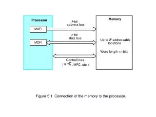
Up to 2
Memory. Processor. k. -bit. address bus. MAR. n. -bit. data bus. k. Up to 2. addressable. MDR. locations. Word length =. n. bits. Control lines. R. /. W. ( , MFC, etc.). Figure 5.1. Connection of the memory to the processor. b. b. ¢. b. b. ¢. b. b. ¢. 7.


Up to 2
E N D
Presentation Transcript
Memory Processor k -bit address bus MAR n -bit data bus k Up to 2 addressable MDR locations Word length = n bits Control lines R / W ( , MFC, etc.) Figure 5.1.Connection of the memory to the processor.
b b ¢ b b ¢ b b ¢ 7 7 1 1 0 0 • • • W 0 FF FF A • • • 0 W 1 A 1 Address Memory • • • • • • • • • • • • • • • • • • cells decoder A 2 A 3 • • • W 15 R / W Sense / Write Sense / Write Sense / Write circuit circuit circuit CS Data input /output lines: b b b 7 1 0 Figure 5.2.Organization of bit cells in a memory chip.
5-bit row address W 0 W 1 32 ´ 32 5-bit memory cell decoder array W 31 Sense / Write circuitry 10-bit address 32-to-1 R / W output multiplexer and CS input demultiplexer 5-bit column address Data input/output Figure 5.3. Organization of a 1K 1 memory chip.
b b ¢ T T 1 2 X Y Word line Bit lines Figure 5.4. A static RAM cell.
Bit line Word line T C Figure 5.6.A single-transistor dynamic memory cell
R A S Row Row 4096 ´ ( 512 ´ 8 ) address decoder cell array latch A ¤ A CS Sense / Write 20 - 9 8 - 0 circuits R / W Column Column address decoder latch C A S D D 7 0 Figure 5.7. Internal organization of a 2M ´ 8 dynamic memory chip.
Refresh counter Row Ro w address Cell array decoder latch Row/Column address Column Co lumn Read/Write address circuits & latches decoder counter Clock R A S Mode register Data input Data output C A S and register register timing control R / W C S Data Figure 5.8.Synchronous DRAM.
Clock R / W R A S C A S Address Row Col Data D0 D1 D2 D3 Figure 5.9.Burst read of length 4 in an SDRAM.
21-bit addresses 19-bit internal chip address A 0 A 1 A 19 A 20 2-bit decoder 512 K ´ 8 memory chip D D D D 31-24 23-16 15-8 7-0 512 K ´ 8 memory chip 19-bit 8-bit data address input/output Chip select Figure 5.10. Organization of a 2M 32 memory module using 512K 8 static memory chips.
Row/Column address Address R A S R / W C A S Memory controller Request R / W Processor Memory C S Clock Clock Data Figure 5.11. Use of a memory controller.
Not connected to store a 1 Connected to store a 0 Bit line Word line T P Figure 5.12.A ROM cell.
Pr ocessor Re gisters Increasing Increasing Increasing size speed cost per bit Primary L1 cache Secondary L2 cache Main memory Magnetic disk secondary memory Figure 5.13.Memory hierarchy.
Main Processor Cache memory Figure 5.14.Use of a cache memory.
Main memory Block 0 Block 1 Block 127 Cache tag Block 0 Block 128 tag Block 1 Block 129 tag Block 127 Block 255 Block 256 Block 257 Block 4095 T ag Block W ord 5 7 4 Main memory address Figure 5.15.Direct-mapped cache.
Main memory Block 0 Block 1 Cache tag Block 0 tag Block 1 Block i tag Block 127 Block 4095 T ag W ord Main memory address 12 4 Figure 5.16. Associative-mapped cache.
Main memory Block 0 Block 1 Cache tag Block 0 Set 0 Block 63 tag Block 1 Block 64 tag Block 2 Set 1 Block 65 tag Block 3 Block 127 tag Block 126 Set 63 Block 128 tag Block 127 Block 129 Block 4095 T ag Set W ord 6 6 4 Main memory address Figure 5.17. Set-associative-mapped cache with two blocks per set.
k bits m bits Module Address in module MM address ABR DBR ABR DBR ABR DBR Module Module Module n - 1 0 i (a) Consecutive words in a module m bits k bits Address in module Module MM address ABR DBR ABR DBR ABR DBR Module Module Module k 2 - 1 0 i (b) Consecutive words in consecutive modules Figure 5.25.Addressing multiple-module memory systems.
Virtual address from processor Page table base register Page table address Virtual page number Offset + PAGE TABLE Control Page frame bits in memory Page frame Offset Physical address in main memory Figure 5.27.Virtual-memory address translation.
Virtual address from processor Virtual page number Offset TLB Virtual page Control Page frame number bits in memory No =? Yes Miss Hit Page frame Offset Physical address in main memory Figure 5.28.Use of an associative-mapped TLB.
Sector 0, track 1 Sector 3, track n Sector 0, track 0 Figure 5.30. Organization of one surface of a disk.
Processor Main memory System bus Disk controller Disk drive Disk drive Figure 5.31. Disks connected to the system bus.