Download
1 / 42
460 likes | 703 Views
Processor and Memory Organisation – Lesson-2 Memory Organisation. 1. ROM. Masked ROM – Used for large scale manufacturing; mask prepared for foundry

E N D
Processor and Memory Organisation – Lesson-2 Memory Organisation Chapter-2 L2: "Embedded Systems - Architecture, Programming and Design" , Raj Kamal, Publs.: McGraw-Hill, Inc.
1. ROM Chapter-2 L2: "Embedded Systems - Architecture, Programming and Design" , Raj Kamal, Publs.: McGraw-Hill, Inc.
Masked ROM – Used for large scale manufacturing; mask prepared for foundry - A finalised ROM image of system program and data, pictograms, image pixels, pixels for the fonts of a language, truth-table implementing combination-circuits Chapter-2 L2: "Embedded Systems - Architecture, Programming and Design" , Raj Kamal, Publs.: McGraw-Hill, Inc.
EPROM – Used in place of masked ROM during development phase; UV Erasable and Electrically programmable by a device programmer Chapter-2 L2: "Embedded Systems - Architecture, Programming and Design" , Raj Kamal, Publs.: McGraw-Hill, Inc.
E2ROM – Used during the program run to save non-volatile data and results (for examples, date and time of a transaction, present port status, port driving history, system malfunctions history); Electrically Erasable by writing a byte with all 1s and Electrically programmable during a program run one byte write at an instance Chapter-2 L2: "Embedded Systems - Architecture, Programming and Design" , Raj Kamal, Publs.: McGraw-Hill, Inc.
Flash – Used during the program run to save non-volatile data and results, for examples, a picture in a digital camera, voice mail; Electrically Erasable sector of 16 kB to 256 kB at an instance and Electrically programmable one byte at an instance during a program run. Chapter-2 L2: "Embedded Systems - Architecture, Programming and Design" , Raj Kamal, Publs.: McGraw-Hill, Inc.
Boot Block Flash – Flash with a sector reserved for programming once only; that sector can be used for saving ROM image or boot program of the system; Exemplary uses: ROM image and OS in mobile phone together with phone book, address book, SMS, MMS Messages Chapter-2 L2: "Embedded Systems - Architecture, Programming and Design" , Raj Kamal, Publs.: McGraw-Hill, Inc.
Memory Stick is a removable flash memory card format. [An 8 GB card was unveiled at a 2006 show at Las Vegas] Exemplary uses: Removable stick in digital camera, Mobile phone, Handheld devices, Handheld compressed voice or video recording in a voice or video recorder Chapter-2 L2: "Embedded Systems - Architecture, Programming and Design" , Raj Kamal, Publs.: McGraw-Hill, Inc.
PROM (OTP) - Used for small scale manufacturing and for saving once only data; used for saving ROM image or boot program of the system and for storing data like user photo and ID and account type and bank details on a card; Chapter-2 L2: "Embedded Systems - Architecture, Programming and Design" , Raj Kamal, Publs.: McGraw-Hill, Inc.
2. RAM • SRAM and DRAM – Used for saving the variables, stacks, process control blocks, input buffer, output buffer, decompressed format of program and data at the ROM image Chapter-2 L2: "Embedded Systems - Architecture, Programming and Design" , Raj Kamal, Publs.: McGraw-Hill, Inc.
EDO (Extended Data Out) RAM – Used up to 100 MHz clock rate, zero wait state between two fetches, single cycle read or write Chapter-2 L2: "Embedded Systems - Architecture, Programming and Design" , Raj Kamal, Publs.: McGraw-Hill, Inc.
SDRAM (Synchronous DRAM) – Synchronised read operation; keeps next word ready while previous one is being fetched; used up to 1 GHz clock cycle Chapter-2 L2: "Embedded Systems - Architecture, Programming and Design" , Raj Kamal, Publs.: McGraw-Hill, Inc.
RDRAM (Rambus* DRAM) – Burst accesses of four successive words in single fetch; used for 1 GHz + performance of the system * A developer company name Chapter-2 L2: "Embedded Systems - Architecture, Programming and Design" , Raj Kamal, Publs.: McGraw-Hill, Inc.
Parameterised Distributed RAM – when slow bus accesses exists RAM distributed for the specific tasks of the system and devices - for examples for fast IO buffers, fast stacks, .. • Parameterised Block RAM – Specific block dedicated for specific use, for example, for DCT operations Chapter-2 L2: "Embedded Systems - Architecture, Programming and Design" , Raj Kamal, Publs.: McGraw-Hill, Inc.
3. Memory Selection Examples Chapter-2 L2: "Embedded Systems - Architecture, Programming and Design" , Raj Kamal, Publs.: McGraw-Hill, Inc.
1.Automatic Washing Machine Needs mass manufacturing therefore masked ROM, needs EEPROM for current machine status, RAM for variables and stack only, A Microcontroller on-chip 256 byte RAM, 4 kB ROM and 128 byte EEPROM suffice [Refer Example 2.6a pp. 69 for details] Chapter-2 L2: "Embedded Systems - Architecture, Programming and Design" , Raj Kamal, Publs.: McGraw-Hill, Inc.
2. Data Acquisition System Data acquired to be stored at the flash (for example 128 kB) ; Needs about 8 kB ROM or EPROM for program memory, 512 B RAM [Refer Example 2.7a pp. 70 for details] Chapter-2 L2: "Embedded Systems - Architecture, Programming and Design" , Raj Kamal, Publs.: McGraw-Hill, Inc.
3. Set-up Box System Large ROM as well as large RAM, 16kB EEPROM for phone and messages memory Chapter-2 L2: "Embedded Systems - Architecture, Programming and Design" , Raj Kamal, Publs.: McGraw-Hill, Inc.
4. Digital camera 1024 color camera images need 64 kB ROM, 32 MB flash, and 1 MB RAM. - Camera with 1 GB memory stick can record image and sound both for several minutes. Chapter-2 L2: "Embedded Systems - Architecture, Programming and Design" , Raj Kamal, Publs.: McGraw-Hill, Inc.
4. Memory Allocation To Program Segments and Blocks Chapter-2 L2: "Embedded Systems - Architecture, Programming and Design" , Raj Kamal, Publs.: McGraw-Hill, Inc.
4.1.Functions, Processes, Data and Stacks at the Various Segments of Memory Segment wise memory allocation in four segments; Code, Data, Stack and Extra (for examples, image, String) Chapter-2 L2: "Embedded Systems - Architecture, Programming and Design" , Raj Kamal, Publs.: McGraw-Hill, Inc.
Segments and Paging at the Memory Chapter-2 L2: "Embedded Systems - Architecture, Programming and Design" , Raj Kamal, Publs.: McGraw-Hill, Inc.
4.2. Different Data Structures at the Various Memory Blocks • Stacks – Return addresses on the nested calls, Sets of LIFO (Last In First Out) retrievable data, Saved Contexts of the tasks as the stacks Chapter-2 L2: "Embedded Systems - Architecture, Programming and Design" , Raj Kamal, Publs.: McGraw-Hill, Inc.
Chapter-2 L2: "Embedded Systems - Architecture, Programming and Design" , Raj Kamal, Publs.: McGraw-Hill, Inc.
Arrays – One dimensional or multidimensional • Queues – Sets of FIFO (First In First Out) retrievable data; Circular Queue (Example- a Printer Buffer); Block Queue (Example- a network stack) Chapter-2 L2: "Embedded Systems - Architecture, Programming and Design" , Raj Kamal, Publs.: McGraw-Hill, Inc.
Chapter-2 L2: "Embedded Systems - Architecture, Programming and Design" , Raj Kamal, Publs.: McGraw-Hill, Inc.
Table • Look up Table – Look-up-table row first column points to another memory block of a data structure data • List: In a list element, a data structure of an item also points to the next item • Process Control Block [Refer Chapter 8 Lesson –1] Chapter-2 L2: "Embedded Systems - Architecture, Programming and Design" , Raj Kamal, Publs.: McGraw-Hill, Inc.
5. Memory Map Map to show the program and data allocation of the addresses to ROM, RAM, EEPROM or Flash in the system Chapter-2 L2: "Embedded Systems - Architecture, Programming and Design" , Raj Kamal, Publs.: McGraw-Hill, Inc.
Chapter-2 L2: "Embedded Systems - Architecture, Programming and Design" , Raj Kamal, Publs.: McGraw-Hill, Inc.
Chapter-2 L2: "Embedded Systems - Architecture, Programming and Design" , Raj Kamal, Publs.: McGraw-Hill, Inc.
Chapter-2 L2: "Embedded Systems - Architecture, Programming and Design" , Raj Kamal, Publs.: McGraw-Hill, Inc.
Chapter-2 L2: "Embedded Systems - Architecture, Programming and Design" , Raj Kamal, Publs.: McGraw-Hill, Inc.
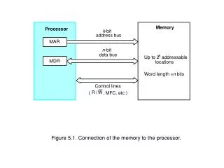
6. Device Addresses Map for Control Register, Status Register, Receive Buffer, Transmit Buffer Device control and status addresses and port address remains constant and are not re-locatable in a program as the glue circuit (hardware) to accesses these is fixed during the circuit design. Chapter-2 L2: "Embedded Systems - Architecture, Programming and Design" , Raj Kamal, Publs.: McGraw-Hill, Inc.
In memory mapped IOs, for example, in 8051 microcontroller, the devices have the addresses for processor-accesses that are not distinct from the memory and are accessed with same set of instructions Chapter-2 L2: "Embedded Systems - Architecture, Programming and Design" , Raj Kamal, Publs.: McGraw-Hill, Inc.
In IO mapped IOs, for example, in 80x86 processor, the devices have the addresses for processor-accesses that are distinct from the memory and are accessed by distinct set of instructions [Refer Example 2.16 for a Serial Line Device on pp. 87-88] Chapter-2 L2: "Embedded Systems - Architecture, Programming and Design" , Raj Kamal, Publs.: McGraw-Hill, Inc.
7. DMA (Direct Memory Access) Controller External Devices can directly write and read into the blocks of RAM using the DMA controller, when the buses are not in use of the processor Chapter-2 L2: "Embedded Systems - Architecture, Programming and Design" , Raj Kamal, Publs.: McGraw-Hill, Inc.
8. Interfacing the processor, memory, devices using a Glue Circuit The processor, memory and devices are interfaced (glued) together using a programmable circuit like GAL or FPGA. The circuit consists of the address decoders as per the memory and device addresses allocated and the needed latches multiplexers/ demultiplexers Chapter-2 L2: "Embedded Systems - Architecture, Programming and Design" , Raj Kamal, Publs.: McGraw-Hill, Inc.
Summary Chapter-2 L2: "Embedded Systems - Architecture, Programming and Design" , Raj Kamal, Publs.: McGraw-Hill, Inc.
We learnt • (i) Various forms of ROM and RAM- masked ROM, PROM, EPROM, EEPROM, flash and boot block flash, SRAM, DRAM, EDO RAM, SDRAM, RDRAM, and parameterised RAMs to enable selection of appropriate memory for an embedded System Chapter-2 L2: "Embedded Systems - Architecture, Programming and Design" , Raj Kamal, Publs.: McGraw-Hill, Inc.
We learnt • (iii) DMA controller, • (iv) Device Addresses and Memory Addresses • (v) Allocations to various Segments and data structures and the memory map, • (vi) Glue Circuit to interface Processor, memory and devices Chapter-2 L2: "Embedded Systems - Architecture, Programming and Design" , Raj Kamal, Publs.: McGraw-Hill, Inc.
We learnt • (vii)Exemplary cases for the estimating the memory requirements Chapter-2 L2: "Embedded Systems - Architecture, Programming and Design" , Raj Kamal, Publs.: McGraw-Hill, Inc.
End of Lesson 2 of Chapter 2 Chapter-2 L2: "Embedded Systems - Architecture, Programming and Design" , Raj Kamal, Publs.: McGraw-Hill, Inc.