Download
1 / 34
340 likes | 450 Views
Extended Memory Controller and the MPAX registers And Cache. Multicore programming and Applications February 19, 2013. Agenda. A little reminder of the 6678 Purpose of MPAX part of XMC CorePac MPAX registers CorePac MAR registers Teranet Access MPAX registers Real code examples

E N D
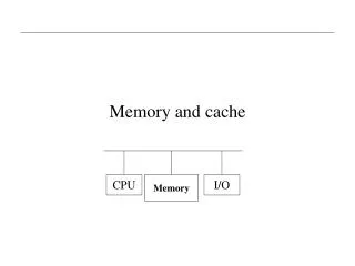
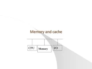
Extended Memory Controller and the MPAX registers And Cache Multicore programming and Applications February 19, 2013
Agenda • A little reminder of the 6678 • Purpose of MPAX part of XMC • CorePac MPAX registers • CorePac MAR registers • Teranet Access MPAX registers • Real code examples • EDMA and cache usage
KeyStone and C66 CorePac 1 to 8 C66x CorePac DSP Cores operating at up to 1.25 GHz Fixed- and floating-point operations Code compatible with other C64x+ and C67x+ devices L1 Memory Can be partitioned as cache and/or RAM 32KB L1P per core 32KB L1D per core Error detection for L1P Memory protection Dedicated L2 Memory Can be partitioned as cache and/or RAM 512 KB to 1 MB Local L2 per core Error detection and correction for all L2 memory Direct connection to memory subsystem Application-Specific Memory Subsystem Coprocessors C66x™ CorePac L1D L1P Cache/RAM Cache/RAM L2 Memory Cache/RAM 1 to 8 Cores @ up to 1.25 GHz Miscellaneous TeraNet HyperLink Multicore Navigator External Interfaces Network Coprocessor
KeyStone I Memory Subsystem • Multicore Shared Memory (MSM SRAM) • 1 to 4 MB • Available to all cores • Can contain program and data • All devices except C6654 • Multicore Shared Memory Controller (MSMC) • Arbitrates access of CorePac and SoCmasters to shared memory • Provides a connection to the DDR3 EMIF • Provides CorePac access to coprocessors and IO peripherals • Provides error detection and correction for all shared memory • Memory protection and address extension to 64 GB (36 bits) • Provides multi-stream pre-fetching capability • DDR3 External Memory Interface (EMIF) • Support for 16-bit, 32-bit, and (for C667x devices) 64-bit modes • Specified at up to 1600 MT/s • Supports power down of unused pins when using 16-bit or 32-bit width • Support for 8 GB memory address • Error detection and correction Application-Specific Memory Subsystem Coprocessors MSM DDR3 EMIF SRAM MSMC C66x™ CorePac L1D L1P Cache/RAM Cache/RAM L2 Memory Cache/RAM 1 to 8 Cores @ up to 1.25 GHz Miscellaneous TeraNet HyperLink Multicore Navigator External Interfaces Network Coprocessor
TeraNet Switch Fabric • A non-blocking switch fabric that enables fast and contention-free internal data movement • Provides a configured way – within hardware – to manage traffic queues and ensure priority jobs are getting accomplished while minimizing the involvement of the CorePac cores • Facilitates high-bandwidth communications between CorePac cores, subsystems, peripherals, and memory Application-Specific Memory Subsystem Coprocessors MSM DDR3 EMIF SRAM MSMC C66x™ CorePac L1D L1P Cache/RAM Cache/RAM L2 Memory Cache/RAM 1 to 8 Cores @ up to 1.25 GHz Miscellaneous TeraNet HyperLink Multicore Navigator Queue Packet Manager DMA t x4 x2 e h T n I c R Security C r P h t e O DeviceSpecific I/O i e DeviceSpecific I/O A c GPIO S I 2 I w Accelerator I h t C U R i t S P w E S S Packet Accelerator I I M x2 G S Network Coprocessor
KeyStone I TeraNet Data Connections TC7 TC4 TC3 TC9 TC2 TC5 TC8 TC6 TC1 TC0 M M M M M M M M M M DebugSS M HyperLink S MSMC DDR3 S M CPUCLK/2 256bit TeraNet S Shared L2 DDR3 HyperLink M M S S S S TPCC 16ch QDMA EDMA_0 • Facilitates high-bandwidth communication links between DSP cores, subsystems, peripherals, and memories. • Supports parallel orthogonal communication links XMC S L2 0-3 M S Core M SRIO M S Core M S Core M M Network Coprocessor M SRIO S TPCC 64ch QDMA S TCP3e_W/R TPCC 64ch QDMA S TCP3d EDMA_1,2 S TCP3d CPUCLK/3 128bit TeraNet S TAC_BE TAC_FE M S RAC_FE RAC_BE0,1 M RAC_FE S RAC_BE0,1 M FFTC / PktDMA M FFTC / PktDMA M S VCP2 (x4) VCP2 (x4) S S VCP2 (x4) AIF / PktDMA M S VCP2 (x4) QMSS M QMSS S PCIe M S PCIe
Memory Translation • All address buses inside CorePac and the Teranet are 32 bit wide • Devices support up to 8GB external memory, requires at least 33 bits (in addition to 2GB of internal memory space) • The solution – translation from logical (32 bit) to physical (36 bit) address. This is done by the Memory Protection and extension/translation unit
MPAX Registers in keyStone devices CorePac Each C66x Core has a set of 16 MPAX 64-bit registers that are used for direct access to the MSMC Each 64-bit register translates a logical segment into physical segment, from 32 bits to 36 bits In addition, the MPAX registers control the access permissions for the memory segment
Structure of the MPAX registers(from the CorePac User Guide) Segment size can be between 4KB to 4GB (power of 2) Permissions are for user mode (read, write, execute) and for supervisor mode (read, write, execute) (Mode is assigned by the operating system, default is supervisor)
The MPAX Address configuration • Each register translates logical memory into physical memory for the segment. • Logical base address (up to 20 bits) is the upper bits of the logical segment base address. The lower N bits are zero where N is determined by the segment size: • For segment size 4K, N = 12 and the base address uses 20 bits. • For segment size 8k, N=13 and the base address uses only 19 bits. • For segment size 1G, N=30 and the base address uses only 2 bits. • Physical (replacement address) base address (up to 24 bits) is the upper bits of the physical (replacement) segment base address. The lower N bits are zero where N is determined by the segment size: • For segment size 4K, N = 12 and the base address uses up to 24 bits. • For segment size 8k, N=13 and the base address uses up to 23 bits. • For segment size 1G, N=30 and the base address uses up to 6 bits.
MPAX: Typical Use Cases • Speeds up processing by making shared L2 MSMC cached by private L2 (L3 shared). • Uses the same logical address in all cores; Each one points to a different physical memory. • Uses part of shared L2 to communicate between cores. So makes part of shared L2 non-cacheable, but leaves the rest of shared L2 cacheable. • Utilizes 8G of external memory; 2G for each core with some over-lapping.
CorePac MPAX Reset Values The XMC configures MPAX segments 0 and 1 so that C66x CorePac can access system memory Segment 0 power up configure it to address all internal memories (up to address 0x7fff ffff) to the same memory The power up configuration is that segment 1 remaps 8000_0000 – FFFF_FFFF in C66x CorePac’s address space to 8:0000_0000 – 8:7FFF_FFFF in the system address map This corresponds to the first 2GB of address space dedicated to EMIF by the MSMC controller
The MPAX Registers System Physical 36-bitMemory Map F:FFFF_FFFF MPAX (Memory Protection and Extension) Registers: • Translate between physical and logical address • 16 registers (64 bits each) control (up to) 16 memory segments. • Each register translates logical memory intophysical memory for the segment. 8:8000_0000 8:7FFF_FFFF 8:0000_0000 7:FFFF_FFFF C66x CorePac Logical 32-bitMemory Map 1:0000_0000 0:FFFF_FFFF MPAX Registers FFFF_FFFF 8000_0000 7FFF_FFFF 0:8000_0000 0:7FFF_FFFF 0:0C00_0000 0:0BFF_FFFF 0C00_0000 0BFF_FFFF Segment 1 Segment 0 0:0000_0000 0000_0000
The protection Part What happen if the application tries to access logical memory that the MPAX register does not have? A fault event will be generated – Software decide what to do
The MAR Registers MAR (Memory Attributes) Registers: • 256 registers (32 bits each) control 256 memory segments: • Each segment size is 16MBytes, from logical address 0x0000 0000 to address 0xFFFF FFFF. • The first 16 registers are read only. They control the internal memory of the core. • Each register controls the cacheability of the segment (bit 0) and the prefetchability (bit 3). All other bits are reserved and set to 0.
CorePac 0 CorePac 1 CorePac 2 CorePac 3 XMC XMC XMC XMC MPAX MPAX MPAX MPAX 256 256 256 256 CorePac CorePac CorePac CorePac Slave Port Slave Port Slave Port Slave Port MSMC Datapath System Slave Port forShared SRAM (SMS) Memory Protection & Extension Unit (MPAX) Arbitration 256 256 TeraNet Shared RAM 2048 KB 256 System Slave Port for External Memory (SES) Memory Protection & Extension Unit (MPAX) Error Detection & Correction (EDC) 256 256 MSMC Core MSMC EMIF MSMC System Master Port Master Port Events 256 256 To SCR_2_B and the DDR TeraNet Teranet and CorePac Access MSMC
A note about Privilege ID in keyStone devices Each C66x Core is assigned a unique privilege ID (PrivID) value Data I/O masters are assigned one PrivID, with the exception of the EDMA, which inherits the PrivID value of the master that configures it for each transfer. There are 16 total PrivID values supported in KeyStone devices.
Access the MSMC from the Teranet (MSMC slave ports) SES (slave port External Memory) access addresses 0x8000 0000 to address 0xffff ffff SMS (slave port Shared SRAM) access addresses 0x0c000 0000 to 0x7fff ffff For access via the TeraNet, there are 16 sets of MPAX registers for System Slave Memory port and 16 sets of MPAX register for System Slave External port. Each set has 8 registers (8 for SES set and 8 for SMS set) Each one set of the 16 sets corresponds to a different Privilege ID .
SES and SMS PMAX Reset Values At reset, the MPAX segment 0 register pair has initial values that set up unrestricted access to the full MSMC SRAM address space and 2 GB of the EMIF address space. All other segments come up with the permission bits and size set to 0 For each PrivID, SMS_MPAXH[0] is reset to 0x0C000017 and SMS_MPAXL[0] is reset to 0x00C000BF, (i.e., segment 0 is sized to 16 MB and matches any accesses to the address range 0x0CXXXXXX). For each PrivID, SES_MPAXH[0] is reset to 0x8000001E and SES_MPAXL[0] is reset to 0x800000BF, (i.e., the segment 0 is sized to 2 GB and matches any accesses to the address range 0x8XXXXXXX). This 2 GB space starts at the external memory base address of 0x80000000. SMS_MPAXH and SMS_MPAXL for segments 1 through 7 come out of reset as 0x0C000000 and 0x00C00000 respectively. SES_MPAXH and SES_MPAXL for segments 1 through 7 come out of reset as all zeros.
Configure the MPAX registers – actual code System Physical 36-bitMemory Map // Map 1 MB from 0x8810_0000 to 0x0_0C00_0000 (XMC) // Use segment 3 – can use any segment lvMpaxh.segSize = 0x13; // 1 MB see table 7-4 lvMpaxh.bAddr = 0x88100; // 32-bit address >> 12 CSL_XMC_setXMPAXH(3,&lvMpaxh); lvMpaxl.ux = 1; lvMpaxl.uw = 1; lvMpaxl.ur = 1; lvMpaxl.sx = 1; lvMpaxl.sw = 1; lvMpaxl.sr = 1; lvMpaxl.rAddr = 0x00C000; // 36-bit address >> 12 CSL_XMC_setXMPAXL(3,&lvMpaxl); F:FFFF_FFFF 8:8000_0000 8:7FFF_FFFF 8:0000_0000 7:FFFF_FFFF C66x CorePac Logical 32-bitMemory Map 1:0000_0000 0:FFFF_FFFF MPAX Registers FFFF_FFFF 881F_FFFF 8810_0000 0:8000_0000 0:7FFF_FFFF 0:0C10_0000 0:0C00_0000 0:0BFF_FFFF 0C00_0000 0BFF_FFFF Segment 1 Segment 0 0:0000_0000 0000_0000
Configure the MPAX registers – actual code // Map 4 KB from 0x2100_0000 to 0x1_0000_0000 (XMC) // Use segment 2 or any other segment lvMpaxh.segSize = 0xB; // 4 KB – see table 7-4 of CorePac lvMpaxh.bAddr = 0x21000; // 32-bit address >> 12 CSL_XMC_setXMPAXH(2,&lvMpaxh); lvMpaxl.ux = 1; lvMpaxl.uw = 1; lvMpaxl.ur = 1; lvMpaxl.sx = 1; lvMpaxl.sw = 1; lvMpaxl.sr = 1; lvMpaxl.rAddr = 0x100000; // 36-bit address >> 12 CSL_XMC_setXMPAXL(2,&lvMpaxl);
Configure MPAX registers for 1GB for each core // Map 1 GB from 0x8000_0000 to 8 different addresses in the external memory // The purpose is to give each core different physical address but have the same logical address lvSesMpaxh.segSz = 0x1D; // 1GB lvSesMpaxh.baddr = 0x2; // 0x8000 0000 32-bit address >> 30 CSL_MSMC_setSESMPAXH(10,2,&lvSesMpaxh); // For each core chose a different setting, start at core 0 lvSesMpaxl.raddr = 0x20; // 8 0000 0000 36-bit >> 30 core 0 lvSesMpaxl.raddr = 0x21; // 8 4000 0000 36-bit >> 30 core 1 lvSesMpaxl.raddr = 0x22; // 8 8000 0000 36-bit >> 30 core 2 lvSesMpaxl.raddr = 0x23; // 8 C000 0000 36-bit >> 30 core 3 … lvSesMpaxl.raddr = 0x27; // 9 C000 0000 36-bit >> 30 core 7 CSL_MSMC_setSESMPAXL(10,2,&lvSesMpaxl);
Configure the SES MPAX registers for Non cached 1M of MSMC shared memory– actual code // Map 1 MB from 0x8800_0000 to 0x0_0C10_0000 (MSMC) // The purpose is to reach MSMC that is not cacheable or pre-fetch //See MAR registers later lvSesMpaxh.segSz = 0x13; lvSesMpaxh.baddr = 0x88100; // 32-bit address >> 12 CSL_MSMC_setSESMPAXH(10,2,&lvSesMpaxh); lvSesMpaxl.ux = 1; lvSesMpaxl.uw = 1; lvSesMpaxl.ur = 1; lvSesMpaxl.sx = 1; lvSesMpaxl.sw = 1; lvSesMpaxl.sr = 1; lvSesMpaxl.raddr = 0x00C000; // 36-bit address >> 12 CSL_MSMC_setSESMPAXL(10,2,&lvSesMpaxl);
Configure the MAR registers – actual code lvMarPtr = (volatile uint32_t*)0x018480030; // MAR12 (0x0C00_0000:0x0CFF_FFFF) // Set MAR attributes for MAR12 lvMar = 1; #ifdef MY_ENABLE_PREFETCH lvMar = lvMar | 8; #endif *lvMarPtr = lvMar;
Configure the MAR registers – actual code // Set MAR attributes for MAR136:MAR143 (0x8800_0000:0x8FFF_FFFF) //This is the region that for (i=0; i<8; i++) { lvMar = 0; *lvMarPtr = lvMar; lvMarPtr++; //CACHE_disableCaching(136+i); }
Internal Buses L1 Memories PC Program Address x32 Fetch Data Address - T1 x32 Program Data x256 A Regs Data Data - T1 x64 L2 and External Memory Data Address - T2 x32 B Regs Data Data - T2 x64 Peripherals
Memory Read Performance SL2 – Configured as Shared Level 2 Memory (L1 cache enabled, L2 cache disabled) SL3 – Configured as Shared Level 3 Memory (Both L1 cache and L2 cache enabled)
Memory Read Performance - Summary Prefetching reduces the latency gap between local memory and shared (internal/external) memories. Prefetching in XMC helps reducing stall cycles for read accesses to MSMC and DDR. Improved pipeline between DMC/PMC and UMC significantly reduces stall cycles for L1D/L1P cache misses. Performance hit when both L1 and L2 caches contain victims Shared memory (MSMC or DDR) configured as Level 3 (SL3) have a potential “double victim” performance impact When victims are in the cache, burst reads are slower than single reads Reads have to wait for victim writes to complete MSMC configured as Level 3 (SL3) is slower than Level 2 (SL2) There is a “double victim” impact DDR configured as Level 3 (SL3) is slower than Level 2 (SL2) in case of L2 cache misses There is a “double victim” impact If DDR does not have large cacheable data, it can be configured as Level 2 (SL2).
Memory Write Performance SL2 – Configured as Shared Level 2 Memory (L1 cache enabled, L2 cache disabled) SL3 – Configured as Shared Level 3 Memory (Both L1 cache and L2 cache enabled)
A word about the EDMA priorities in 6678 Choose the right edma controller (connectivity, location, clock, width) In each channel controller, choose the right channel (lower channel number higher priorities) and transfer controller (The same) The FIFO size determine the amount of overhead to choose the right TC Consider parallel events and blocking