Download
1 / 4
40 likes | 201 Views
The interplay of orbital and spin degrees of freedom in nanosystems Materials World Network (USA – Brazil – Chile) George B. Martins, Oakland University, DMR 0710529.

E N D
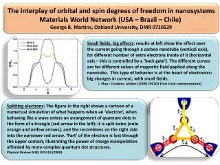
The interplay of orbital and spin degrees of freedom in nanosystems Materials World Network (USA – Brazil – Chile) George B. Martins, Oakland University, DMR 0710529 Small fields, big effects: results at left show the effect over the current going through a carbon nanotube (vertical axis), for different number of extra electrons inside of it (horizontal axis – this is controlled by a ‘back gate’). The different curves are for different values of magnetic field applied along the nanotube. This type of behavior is at the heart of electronics: big changes in current, with small fields. J. Phys.: Condens. Matter (2009) 292203 (Fast track communication). Splitting electrons: The figure in the right shows a cartoon of a numerical simulation of what happens when an ‘electron’, when behaving like a wave enters an arrangement of quantum dots in the form of a triangle (red arrow in the left): it is split twice (note orange and yellow arrows), and the recombines on the right side into the narrower red arrow. ‘Part’ of the electron is lost through the upper contact, illustrating the power of charge manipulation afforded by more complex quantum dot structures. Physical Review B 80, 035119 (2009)
What are clouds made of? Materials World Network (USA – Brazil – Chile) George B. Martins, Oakland University, DMR 0710529 What is around a spin?: results on the left (see inset, with change in the density of states) show the extent of the perturbation caused by a spin, over its neighborhood, when clothed by a ‘cloud’ of other spins, which try to screen (suppress) it. The decay of the perturbation (main panel) is shown to be exponential. Submitted to PRB. Cloud’s size: The extent of this perturbation (right), denoted by RK, varies inversely with the coupling of the spin to the other electrons (Δ). The reason being that the less the other electrons can ‘see’ the spin, the more of them are needed to screen it, the larger is the cloud… • The cloud inside-out: A more detailed analysis of the ‘cloud’ shows many interesting features: • The behavior of the perturbation over the ‘screening’ electrons has two different regimes: ‘inside’ the cloud the perturbations decays as N1/2, while ‘outside’, the decay depends on N-1. • The transition between the two regimes, obviously, gives a good estimate of the ‘size’ of the cloud. As these two different regimes can, in principle, be detected experimentally, one would be able to probe this elusive strongly correlated state. • Submitted to Phys. Rev. B
Dr. Nikola Tesla comes to town Materials World Network (USA – Brazil – Chile) George B. Martins, Oakland University, DMR 0710529 With the intent of creating a group of students that can perform physics presentations at high schools and captivate their audience (teenagers), some of the undergrad Oakland students, accompanied by Dr. Martins, went to Troy High (in Michigan) in April 2009 and presented a whole set of demos centered around the work of Dr. Nikola Tesla. In reality, Dr. Nikola Tesla (Oakland University physics undergrad student Andrew Poterek – at right) was so excited about the idea that he himself decided to take part in the final demonstration of his Tesla Coil!! Andrew dyed his hair (he is actually blond), sported a fake mustache, and we went to the Drama Department and found the appropriate costume for the epoch (hat, cane, and suit are not shown here). This demonstrates the level of commitment of the students involved in this outreach project. We had the opportunity of talking to the students about the Physics career and the wonders of nanotechnology. The turn out exceeded expectations and the team (4 students) is booked for presentations until next year!! Including one for a regional group of Physics high-school teachers, to be held at Oakland, in October 2009. Oakland University physics student, Andrew Poterek, aka Dr. Nikola Tesla, discussed many aspects of the functioning of his famous Tesla Coil. At left, he is showing physics high-school students, a noble gas lamp being activated by the strong electric fields generated by his apparatus. Dr. Tesla was ‘brought back’ to life just for this one presentation, however, he (and the students) enjoyed it so much that he decided to ‘stick around’ for a bit longer and perform again. Dr. Tesla was accompanied by 3 of his lab assistants. At the end of his presentation, he asked the students to sign a petition in favor of transforming his Wardenclyffe laboratory in New York into a museum. The students were all enthusiastic about giving him a hand.
A bridge across the continent Materials World Network (USA – Brazil – Chile) George B. Martins, Oakland University, DMR 0710529 A webpage with content related to our USA-Brazil-Chile collaboration is being hosted at Oakland University (http://www2.oakland.edu/ciam/). This webpage contains some outreach work, which will be extended in the remaining years of this grant. Besides the posting of the majority of the talks presented at the workshop in Chile (January – 2009), it also contains a list of articles discussing the relevance of the efforts being developed in Latin America to invest in research related to nanoscience, and in activities that may result in an integration of industry and universities in this field. In addition, our wikipage is now being more frequently used. Collaborators in all three countries involved are starting to take advantage of what it has to offer. The wiki has been an important instrument, in combination with skype, for the quick interchange of ideas. In the standard use, members of the collaboration can discuss via skype while at the same time edit documents on the wiki. The person on the other side sees the updates on the material, in real time. The final version of the updated document is saved and the site serves as a database for different projects that greatly facilitates (and democratizes) the access to information in each project. The wiki is very easy to update and maintain (once the cyber-security requirements of each University are met). Once a project is ‘finished’, the wiki provides an organized source of text, graphs, and comments (including bibliographic information) for the production of a paper to be submitted. Our wiki can be accessed at http://victom.oakland.edu:441/mwnwiki/ (note that a password is required to enter it).