Array-Based Architecture for FET-Based, Nanoscale Electronics
Array-Based Architecture for FET-Based, Nanoscale Electronics. Andr é DeHon 2003. Presented By Mahmoud Ben Naser. Move to Nanotechnology. CMOS size limits Cost of Fabrication. Source: Kahng/ITRS2001. Differences with current technology. CMOS Top Down construction

Array-Based Architecture for FET-Based, Nanoscale Electronics
E N D
Presentation Transcript
Array-Based Architecture for FET-Based, Nanoscale Electronics André DeHon 2003 Presented By Mahmoud Ben Naser
Move to Nanotechnology • CMOS size limits • Cost of Fabrication Source: Kahng/ITRS2001
Differences with current technology CMOS • Top Down construction • Precise placement of devices Nanotechnology • Bottom Up construction • Stochastic assembly.
Building Blocks (Wires) • Carbon Nanotubes (CNTs or NT) • Silicon NanoWires (SiNW or NW)
Carbon Nanotube • Built by “exploding” carbon or carbon vapor. • Can be conducting or semiconducting • A few nm diameter • Can’t selectively manufacture one type or the other.
Silicon Nanowires • “Grown” by vapor deposition • Precise diameter control of a few nm • Microns long • Selectively dope length to control electrical properties
Devices (Switches) • CNT Suspended Memories • Molecular Switches • SiNW FET
CNT switches • CNTs in parallel suspended above perpendicular set of CNTs
SiNW • Core Shell NW • Gated by NT or NW Diode FET
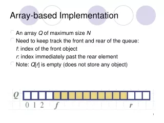
Architecture Using building blocks and switches what can we build? • Crossbar Arrays • Memory, PLA, or Interconnect • Collection of small arrays to exploit logical structure and isolate faults
Electrical Operation Diode Logic • NW or NT crosspoint directly touching • Wired-OR • Programmable Junction • Problem: Non-restring
Electrical Operation • FET Logic (PFET) • Problems: • Generally Non-Programmable Logic • Static Power Consumption
Using the Crossbar Array • Connect to the microworld without loosing gains from nano-pitch • Program junctions
Addressing individual NWs • Can’t connect a mW to each NW. • Use a nanodecoder with 2-hot addressing (minimize the effect fault on address line). To Crossbar Array
Nano-Decoder Evaluation • Advantage: Precise predefined codeset • Only loose Sqrt(n) wires on address fault • Disadvantage: Hard to create nano-imprint pattern • Use axially doped NW instead
Big Picture 4 Decoders 2 Decoders Can disable decoders if needed during operation
Programmable FET Arrays • Using Core-Shelled NWs on the bottom and NTs on the top. • During operation use decoder as pull up or pull down network.
Crosspoint Density • Decoders add a lot of overhead, is it still worth it to “go nano”? • Still do better then CMOS bit-density. Can easily achieve 50% of core density.
Defect Tolerance Types of defects • Broken wire • Defective crosspoint • Defective array • Add Redundancy
Broken Wire • Components fully interchangeable • Rout around defect.
Defective Crosspoints • HP calculates 15% of crospoints “Stuck” • Use algorithm to successfully rout around this
Defective Array • Though more unlikely, it’s possible. • Ensure availability of more resources to completely rout around the array.
Effects of Defects • Look at expected yield of address decoder and multiply by expected yield of crossbar array. • Both dependant on design model chosen • Type of codes used in decoder • Building block used
Conclusion • Nanoelectronic systems provide several advantages over conventional silicon, most importantly increased density. • Because of their extremely small size, nanoscale devices present new problems in fabrication and fault tolerance that must be overcome. • must be able to interface with conventional silicon chips, at least in the short run.