Download
1 / 55
580 likes | 800 Views
George J. Kostas Nanoscale Technology and Manufacturing Research Center www.kostas.neu.edu. Fabrication and Characterization Facilities at the George J. Kostas Nanoscale Technology and Manufacturing Research Center Richard DeVito, Operating Director

E N D
George J. Kostas Nanoscale Technology and Manufacturing Research Center www.kostas.neu.edu Fabrication and Characterization Facilities at the George J. Kostas Nanoscale Technology and Manufacturing Research Center Richard DeVito, Operating Director George J. Kostas Nanoscale Technology and Manufacturing Research
Outline • Introduction • Characterization Capabilities • Fabrication Capabilities • User Training And Access • Summary
The George J. Kostas Nanoscale Technology and Manufacturing Research Center is the primary facility for micro and nanofabrication at Northeastern University. Established through Mr. George J. Kostas '43 generous gift, The facility was completed in January 2005. • The Kostas facility also serves as the main facility for the new NSF Nanoscale Science and Engineering Center for High-rate Nanomanufacturing (CHN) at Northeastern University, in partnership with the University of Massachusetts Lowell, and the University of New Hampshire . • The facility is open to faculty, students, researchers, coop students, and external users. The facility provides support and materials based on user fees and has capabilities for processing 3,4, and 6 inch wafers as well as smaller parts. Fabrication and Characterization Facilities at the George J. Kostas Nanoscale Technology and Manufacturing Research Center
The center consists of 5000 square feet of class 10, 1000, and 10000 clean room space Fabrication and Characterization Facilities at the George J. Kostas Nanoscale Technology and Manufacturing Research Center
Lithography – Optical, Electron Beam Deposition PVD; CVD; TVD; EBE; Electroplating Etching Dry Etch; RIE Bonders and Flip Chip Aligner Cleaning Ultrasonic; Megasonic; Wet bench Surface Analysis Profile Analysis Energy Dispersive Analysis Thickness Analysis V-I Characterization Surface Scanner Zeta potential measurement Fabrication and Characterization Fabrication Characterization
Employs Scattering cross-section of laser Light • is 632.8nm Can detect particles down to 200nm. 4” to 6” wafer sizes Tencor Laser Surface Scanner
Nikon Optiphot 200D Microscope with a fluorescent attachment Excitation ~ 542 nm Emission ~ 612 nm Detect particles 180X Zoom Surface Analysis – Optical Microscopes
Contact Angle Analyzer: SEO • Max. Size 6 inch • Automatic and rapid sample analysis • High-speed dynamic image capture • Improved precision and reproducibility • Measurement of surface tension and static/dynamic contact angle. • Calculation of surface energy and work of adhesion.
Capability: • Resolution: 1 nm @ 30kV; 3.5 nm @ 1 kV • Magnification: 12 - 500,000x • Acc Voltage: 0.2-30kV • Probe Current: 24pA-10nA • Detectors: Secondary In lens (0.2-20kV) • EHT (0.2kV-30kV) Surface Analysis, FESEM, Supra-25
30 Second Cool down utilizing air-cooled Peltier cooling Operating Temperature 115° C No moving parts No vibration Signal shaping and resolution specification at 1 microsecond EDS Analysis – PGT EDS Detector
When monochromatic radiation is incident upon a sample then this light will interact with the sample in some fashion. It may be reflected, absorbed or scattered in some manner. It is the scattering of the radiation that occurs which can tell the Raman spectroscopist something of the samples molecular structure. Rayleigh Raman SpectroscopyJobinYvon Lab Ram HR 800 Raman • The scattering process without a change of frequency is called Rayleigh scattering, • A change in the frequency (wavelength) of the light is called Raman scattering. Raman shifted photons of light can be either of higher or lower energy, depending upon the vibrational state of the molecule. • The Lab Ram has two excitation laser wavelengths of 532 and 785 nm • Band analysis in the order of 0.3cm-1 to 1cm-1 is particularly suited to the HR mode
X-Ray DiffractionPanalytical X’Pert Pro • 1.8kW sealed X-ray tube source, • Cu target • vertical circle theta goniometer with a radius of 240mm • rocking curve analysis and reciprocal space mapping • reflectometry and thin film phase analysis • residual stress and texture analysis
Surface Profile analysis Sputtered Ti Profile Analysis – Park Scientific NX10 AFM
Salient Features: • Separated X-Y & Z Scanner • Nanolithography • Fluid cell: Supports all major SPM functions • XY Motorized Stage • EZ Snap Probe Tip Exchange • Low Noise XE System Controller Surface Profile analysis of Patterned Resists Profile Analysis – PSIA -XE150 SPM
Typical Profile analysis result • Step Profile for Nonmetals & Standard Metal • 500A to 50m Surface Profile Analysis – DEKTAK 3030
• Fast noncontact measurements • • Sub-nanometer Z resolution • • Leading-edge precision • & gage capability • • Enhanced optical imaging • Various surfaces: opaque, • transparent, coated, uncoated, • specular, and nonspecular • Vertical Scan Range 150 μm • Vertical Res. Up to 0.1 nm • Lateral Res. 0.43 to 11.6 μm ZYGO NewView 6200Optical Profilometer
NanoSpec • Thickness measurement for Multilayer transparent films on Si • Max.wafer size 4 inch and max. thickness 1.5 m Thickness Analysis Non-contact, Spectro-Reflectometry
Inline Four Probe Method HP system for V-I Characterization of ICs V-I Characterization – Microprobes
Varian Cary 300 Spectrophotometer • Wavelength Range: • 190-900 nm • UV WinlabSoftware Controlled • Spectral Bandwidth • 0.2-4 nm in 0.1 nm steps • Wavelength Accuracy: • +/-.02 nm • Wavelength Reproducibility: • +/- 0.008 nm • Scan Rate(Max) • 3000 nm /min • Photometric Range • 6 Abs
Janis ST 500 Electrical Probe Station Electrical sample characterization in high vacuum or air or inert atmosphere. sample temperature 4-420 K with LHe Probe sizes down to 7 microns. It has 4 x-y-z probes and 4 triax connectors on these probes. Frequency response is DC to 10 MHz. It also had the ability to apply a magnetic field using permanent magnets in plane and parallel at 1000 Gauss The system is mounted on a vibration isolation mount and has a CCTV camera mounted to Lieca zoom microscope (not shown) V-I Characterization – Microprobes IILow Temperature/ High Vacuum
• Mechanical and electrical characterization.• Device quality/failure analysis.• Nanostructure/nanomaterial /nanointerconnect R&D.• MEMS/IC or microstructure R&D.• Surface science experiments.• Assembly and manipulation. Zyvex Nanomanipulator S-100
Fully Automated Full ph range Only for aqueous solutions Min. weight percent 1 Zeta Potential Measurement
Spinner Baking Ovens Hotplates Photo resist Baking Spinner Vacuum Optical Lithography
Optical Exposure Ultra violet light Optical Mask After Development • Quintel4000 Optical Aligner • Infra Red Mask alignment • 6 & 3 inch wafers Optical Lithography Limitations :l determines the min. pattern width
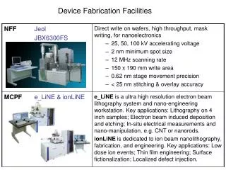
De Broglie Hypothesis Electron Beam Lithography • Nano pattern Generation System (NPGS) • Capability down to 15nm patterns • Continuous Pattern Writing for 45hours • Control of the SEM using REMCON32 • Auto alignments and focus for tilt and stage movements • Raith Beam Blanker • Electrostatic Beam Blanker • Operating Frequency is 100 kHz FESEM- Carl Zeiss Surpa25
Nanonex NX200 Nano-imprinter Nano Imprint LithographyNanonexNX 200
Focused Ion Beam (FIB) Zeiss Cross Beam™ 1540XB (dual beam) • Resolution Electron-Beam1 nm at 20 kV at WD = 2 mm. • Resolution Ion-Beam7 nm (5 nm achievable) • Magnification12x - 900,000x (SEM) • Ion SourceUHV, with Gallium liquid metal ion source • The 1540 is a high performance instrument designed for micro structural sectioning, imaging and analytical applications. The system features unique GEMINI® electron optical column technology and the new Canion 31 FIB column. The 1540XB benefits the user with its flexible handling of a variety of sample types and sizes with a 6-axes motorised high precision super-eucentric stage
Permanent Magnets Target H RF Field • Perkin Elmer 2400 • Three 8” Target • RF & DC Magnetron • Sputtering Patterned Resist Ar Gas Substrate Deposition – PVD • Mat Vac 8667 • 3 x 6.5” Targets • RF/DC Sputtering Available Targets: Al, Ni, In2O3/SNO2, Mo, Cu, Ti, Si, Si3N4, NiCr, C, Cr, TiW, Au, Ru
Up to 4” diameter substrates Water cooled substrate holder Two boat deposition Qualified for Cr, Au, MgF2,Ag,Al Deposition – Thermal Evaporation
4 pocket-6c.c.crucible/ e-beam deposition system can accept up to 4" substratesAvailable Material (Metals Only) • Ti - Titanium • Cr - Chromium • Au - Gold • Al - Aluminum • Ni - Nickel Deposition – E-Beam Evaporation
Deposition – PECVDAstex LL System SiOx, SiN2 • ECR Electron Cyclotron Resonance • High density electron • SiNx without NH3 • Down stream Plasma Deposition • 5-10 mtorr pressure • Long MFP • Excellent Uniformity • Low Damage energetics at substrate
t = Time period • N = Number of electrons for stability • = density e = Electronic Charge a = Area T = Thickness A = Atomic Weight I = current V Substrate Target Patterned Resist Available Electrolyte: Au, Zn Electrolytic solution Deposition – Electroplating
Heat Substrate Chemicals Dry Oxidation Wet oxidation Polysilicon deposition Silicon Nitride deposition Silicon Oxide deposition Bruce Furnace with 4 and 6 inch Stacks Deposition – Oxidation
Annealing FurnaceMiniBrute • 4” tube • 3” substrates • 400 C • Inert or H2 atmosphere
MEI 1204 B Hybrid Ball Bonder Bonding Area ~100 m X 100 m Bonding Metal Au Wire BondersMEI 1204B Ball Bonder
Substrate Heat Deposition – TVD, PDS2010 Biocompatibility Truly conformal material (pin-hole free at 25 nm thickness) Thin film dielectric Excellent moisture/chemical barrier properties High mechanical strength
Dry Etching – Ion Beam Milling Vecco MicroEtch 10” Ion Beam Milling System Acc. Voltage 1kV Shutter Current ~1Amp
XACTIX e1™ SeriesXeF2 Silicon Etch System • The e1 uses XeF2 as the etching gas. Xenon difluoride exhibits a high selectivity to silicon versus many materials. • Xenon Difluoride Advantages • Selectivity during etchingXeF2 shows very high selectivity vs silicon to the majority of semiconductor materials including photoresist, silicon dioxide, silicon nitride, and aluminum. Typically the selectivity of silicon nitride is better than 100:1 and the selectivity to silicon dioxide is better than 1000:1. • No release stictionXeF2 etching is a dry process so no drying is needed which avoids the sticking issues that often plague wet release processes. • Delicate structures are safely releasedSince XeF2 etching is a dry, room temperature process delicate structures can be released. This is particularly useful for releasing delicate devices, such as micromirrors, that are best released after dicing and wire bonding.
Oxford InstrumentsPlasma Pro 100 ICP Etch System • Load Locked ICP etch system (inductively coupled plasma) • ICP source produces a high density of reactive species at low pressure. Substrate bias controlled by separate RF source, allowing independent control of ion energy • Uses CL2 and BCL3 etch gases • Back Side Helium cooling • Up to 6” capability RF1 RF2
RF Field 2 RF Field 1 ICP Plasma Therm 790 Patterned Resist Available Gases: SF6, Ar, O2 Chemical Gas Substrate Dry Etching – ICP
Anatech SP-100 Asher • Used for removal of PR,PMMA • Plasma de-scum post development prior to deposition • Low temp inductively coupled plasma
Cleaning – Wet Benches H2O2/H2SO4 (1:2) Removal of some metals & Organic materials H2O/H2O2/H2SO4 (1:1:6) Removal of metals HF/H2O (1:50) Removal of Oxide layer
n Viscosity w Frequency Cleaning – Ultrasonic
n Viscosity w Frequency Cleaning – Megasonic
Glove BoxInnovative Technology Inc. • Single glove box with Spinner and hot plate • N2/Ar atmosphere • 1 ppm O2 background • PLC controlled
Wafer DicingMicroAutomation1006A Dicing Saw • Dicing of semiconductor wafers • Silicon or glass • Up to 6” capability