Metal oxide semiconductor capacitor MOS capacitor
660 likes | 1.59k Views
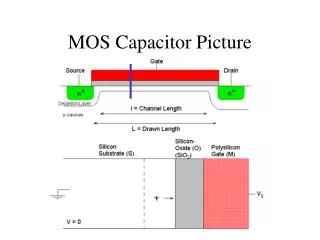
Metal oxide semiconductor capacitor MOS capacitor. MOS capacitor before joining. The metallic gate may be replaced with a heavily doped p+ polysilicon gate. The Fermi energy levels are approximately at the same level. Positive electron energy. MOS capacitor before joining.

Metal oxide semiconductor capacitor MOS capacitor
E N D
Presentation Transcript
Metal oxide semiconductor capacitor MOS capacitor
MOS capacitor before joining The metallic gate may be replaced with a heavily doped p+ polysilicon gate. The Fermi energy levels are approximately at the same level.
Positive electron energy MOS capacitor before joining
MOS capacitor after joiningAssume that there is no charge in the oxide layer
V G MOS capacitor p type semiconductorvoltage bias effects - - - - E + + + +
V G MOS capacitor p type semiconductorvoltage bias effects –battery switched + + + + E - + - + - + - +
V G MOS capacitor n type semiconductorvoltage bias effects + + + + E - - - -
V G MOS capacitor n type semiconductorvoltage bias effects –battery switched - - - - E + - + - + - + -
MOS capacitor after joiningAssume that there is charge in the oxide layer
V G MOS capacitor p type semiconductor gate voltage VG = VFlatband Charge No depletion layer No bending
V G MOS capacitor p type semiconductor gate voltage VG = VT “threshold” Charge Inversion layer
MOS capacitor –charge distribution . . Charge separation yields a capacitance
Problem 6.1 Charge distributions are depicted in an MOS capacitor. 1) Is the semiconductor n or p type? 2) Does the bias make it an accumulation mode, depletion mode or an inversion mode? P type Inversion P type depletion
Problem 6.1 Charge distributions are depicted in an MOS capacitor. 1) Is the semiconductor n or p type? 2) Does the bias make it an accumulation mode, depletion mode or an inversion mode? n type inversion P type accumulation
Electric field due to charges Assume Boundary condition
MOS capacitor – changing charge distribution with changing voltageaccumulation mode . .
MOS capacitor – changing charge distribution with changing voltagedepletion mode . .
MOS capacitor – changing charge distribution with changing voltage
MOS capacitor – changing charge distribution with changing voltage veractor -- vericap
definition Approximate proportion of charge located at x
Problem 6.22 Using superposition, find the dependence of the “flat bad voltage” as the charge density changes. Nonuniform charge density @ x Change of flat band voltage Superimposition applies
Problem 6.23 Using superposition, find the dependence of the “flat bad voltage” for a particular charge density profiles.. Charges located just at the interface
Problem 6.23 Using superposition, find the dependence of the “flat bad voltage” for a particular charge density profiles.. Charge density is nonuniform
Problem 6.28 Consider the high-frequency capacitance-voltage relationship. Locate the inversion; threshold; depletion; flat band, and accumulation points.