Download
1 / 31
310 likes | 325 Views
inst.eecs.berkeley.edu/~cs61c CS61C : Machine Structures Lecture #18 Single Cycle CPU Control 2005-11-02. There is one handout today at the front and back of the room!. CPS today!. Lecturer PSOE, new dad Dan Garcia www.cs.berkeley.edu/~ddgarcia.

E N D
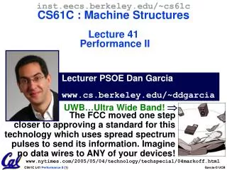
inst.eecs.berkeley.edu/~cs61cCS61C : Machine StructuresLecture #18Single Cycle CPU Control2005-11-02 There is one handout today at the front and back of the room! CPStoday! Lecturer PSOE, new dad Dan Garcia www.cs.berkeley.edu/~ddgarcia Data Transfer Record!A Japanese company(Kansai Electric) claims fiber-optic cables on power-transmitting steel towers have achieved 1 Terabit/sec, 100 times faster than normal. 5:00:00 send 2 hr movie 5:00:01 get 2 hr movie(< 1 second!) news.softpedia.com/news/Japanese-Claim-New-Fiber-Optic-Transmission-Record-11257.shtml
Instruction<31:0> nPC_sel Instruction Fetch Unit Rd Rt <0:15> <21:25> <16:20> <11:15> Clk RegDst 1 0 Mux Rt Rs Rd Imm16 Rs Rt RegWr ALUctr Zero 5 5 5 MemWr MemtoReg busA Rw Ra Rb busW 32 32 32-bit Registers 0 ALU 32 busB 32 0 Clk 32 Mux Mux 32 1 WrEn Adr 1 Data In 32 Data Memory imm16 Extender 32 16 Clk ALUSrc ExtOp Summary: A Single Cycle Datapath • Rs, Rt, Rd, Imed16 connected to datapath • We have everything except control signals
PC ALU Clk An Abstract View of the Critical Path Critical Path (Load Operation) = Delay clock through PC (FFs) + Instruction Memory’s Access Time + Register File’s Access Time, + ALU to Perform a 32-bit Add + Data Memory Access Time + Stable Time for Register File Write • This affects how much you can overclock your PC! Ideal Instruction Memory Instruction Rd Rs Rt Imm 5 5 5 16 Instruction Address A Data Address 32 Rw Ra Rb 32 Ideal Data Memory 32 32 32-bit Registers Next Address Data In B Clk Clk 32
nPC_MUX_sel Inst Memory Adr 4 Adder 00 Mux PC Adder Clk imm16 PC Ext Recap: Meaning of the Control Signals • nPC_MUX_sel: 0 PC <– PC + 4 1 PC <– PC + 4 + {SignExt(Im16) , 00 } • Later in lecture: higher-level connection between mux and branch cond “n”=next
Recap: Meaning of the Control Signals • MemWr: 1 write memory • MemtoReg: 0 ALU; 1 Mem • RegDst: 0 “rt”; 1 “rd” • RegWr: 1 write register • ExtOp: “zero”, “sign” • ALUsrc: 0 regB; 1 immed • ALUctr: “add”, “sub”, “or” RegDst ALUctr MemWr MemtoReg Equal Rt Rd 0 1 Rs Rt RegWr 5 5 5 busA = Rw Ra Rb busW 32 32 32-bit Registers ALU 0 32 busB 32 0 32 Mux Mux Clk 32 WrEn Adr 1 1 Data In Data Memory imm16 Extender 32 16 Clk ExtOp ALUSrc
31 26 21 16 11 6 0 op rs rt rd shamt funct 6 bits 5 bits 5 bits 5 bits 5 bits 6 bits RTL: The Add Instruction add rd, rs, rt • MEM[PC] Fetch the instruction from memory • R[rd] = R[rs] + R[rt] The actual operation • PC = PC + 4 Calculate the next instruction’s address
Inst Memory Adr Adder Mux Adder Instruction Fetch Unit at the Beginning of Add • Fetch the instruction from Instruction memory: Instruction = MEM[PC] • same for all instructions Instruction<31:0> nPC_MUX_sel 4 00 PC Clk imm16 PC Ext
31 26 21 16 11 6 0 op rs rt rd shamt funct The Single Cycle Datapath during Add • R[rd] = R[rs] + R[rt] Instruction<31:0> nPC_sel= +4 Instruction Fetch Unit Rd Rt <21:25> <16:20> <11:15> <0:15> Clk RegDst = 1 1 0 Mux ALUctr = Add Rt Rs Rd Imm16 Rs Rt RegWr = 1 5 5 5 MemtoReg = 0 busA Zero MemWr = 0 Rw Ra Rb busW 32 32 32-bit Registers 0 ALU 32 busB 32 0 Clk Mux 32 Mux 32 1 WrEn Adr 1 Data In 32 Data Memory Extender imm16 32 16 Clk ALUSrc = 0 ExtOp = x
Inst Memory Adr Adder Mux Adder Instruction Fetch Unit at the End of Add • PC = PC + 4 • This is the same for all instructions except: Branch and Jump Instruction<31:0> nPC_MUX_sel 4 00 0 PC 1 Clk imm16
31 26 21 16 0 op rs rt immediate Single Cycle Datapath during Or Immediate? • R[rt] = R[rs] OR ZeroExt[Imm16] Instruction<31:0> nPC_sel = Instruction Fetch Unit Rd Rt <0:15> <21:25> <16:20> <11:15> Clk RegDst = 1 0 Mux Rt Rs Rd Imm16 Rs Rt ALUctr = RegWr = 5 5 5 MemtoReg = busA Zero MemWr = Rw Ra Rb busW 32 32 32-bit Registers 0 ALU 32 busB 32 0 Clk Mux 32 Mux 32 1 WrEn Adr 1 Data In 32 Data Memory Extender imm16 32 16 Clk ALUSrc = ExtOp =
31 26 21 16 0 op rs rt immediate Single Cycle Datapath during Or Immediate? • R[rt] = R[rs] OR ZeroExt[Imm16] Instruction<31:0> nPC_sel= +4 Instruction Fetch Unit Rd Rt <0:15> <21:25> <16:20> <11:15> Clk RegDst = 0 1 0 Mux Rt Rs Rd Imm16 Rs Rt ALUctr = Or RegWr = 1 MemtoReg = 0 5 5 5 busA Zero MemWr = 0 Rw Ra Rb busW 32 32 32-bit Registers 0 ALU 32 busB 32 0 Clk Mux 32 Mux 32 1 WrEn Adr 1 Data In 32 Data Memory Extender imm16 32 16 Clk ALUSrc = 1 ExtOp = 0
31 26 21 16 0 op rs rt immediate The Single Cycle Datapath during Load? • R[rt] = Data Memory {R[rs] + SignExt[imm16]} Instruction<31:0> nPC_sel= Instruction Fetch Unit Rd Rt <21:25> <16:20> <11:15> <0:15> Clk RegDst = 1 0 Mux ALUctr = Rt Rs Rd Imm16 Rs Rt RegWr = MemtoReg = 5 5 5 busA Zero MemWr = Rw Ra Rb busW 32 32 32-bit Registers 0 ALU 32 busB 32 0 Clk Mux 32 Mux 1 WrEn Adr 1 Data In 32 Data Memory Extender 32 imm16 32 16 Clk ALUSrc = ExtOp =
31 26 21 16 0 op rs rt immediate The Single Cycle Datapath during Load • R[rt] = Data Memory {R[rs] + SignExt[imm16]} Instruction<31:0> nPC_sel= +4 Instruction Fetch Unit Rd Rt <21:25> <16:20> <11:15> <0:15> Clk RegDst = 0 1 0 Mux ALUctr = Add Rt Rs Rd Imm16 Rs Rt RegWr = 1 MemtoReg = 1 5 5 5 busA Zero MemWr = 0 Rw Ra Rb busW 32 32 32-bit Registers 0 ALU 32 busB 32 0 Clk Mux 32 Mux 1 WrEn Adr 1 Data In 32 Data Memory Extender 32 imm16 32 16 Clk ALUSrc = 1 ExtOp = 1
31 26 21 16 0 op rs rt immediate The Single Cycle Datapath during Store? • Data Memory {R[rs] + SignExt[imm16]} = R[rt] Instruction<31:0> nPC_sel = Instruction Fetch Unit Rd Rt <0:15> <21:25> <16:20> <11:15> Clk RegDst = 1 0 Mux Rt Rs Rd Imm16 Rs Rt ALUctr = RegWr = 5 5 5 MemtoReg = busA Zero MemWr = Rw Ra Rb busW 32 32 32-bit Registers 0 ALU 32 busB 32 0 Clk Mux 32 Mux 32 1 WrEn Adr 1 Data In 32 Data Memory Extender imm16 32 16 Clk ALUSrc = ExtOp =
31 26 21 16 0 op rs rt immediate The Single Cycle Datapath during Store • Data Memory {R[rs] + SignExt[imm16]} = R[rt] Instruction<31:0> nPC_sel= +4 Instruction Fetch Unit Rd Rt <0:15> <21:25> <16:20> <11:15> Clk RegDst = x 1 0 Mux ALUctr = Add Rt Rs Rd Imm16 Rs Rt RegWr = 0 5 5 5 MemtoReg = x busA Zero MemWr = 1 Rw Ra Rb busW 32 32 32-bit Registers 0 ALU 32 busB 32 0 Clk Mux 32 Mux 32 1 WrEn Adr 1 32 Data In Data Memory Extender imm16 32 16 Clk ALUSrc = 1 ExtOp = 1
31 26 21 16 0 op rs rt immediate The Single Cycle Datapath during Branch? • if (R[rs] - R[rt] == 0) then Zero = 1 ; else Zero = 0 Instruction<31:0> nPC_sel= Instruction Fetch Unit Rd Rt <0:15> <21:25> <16:20> <11:15> Clk RegDst = 1 0 Mux Rt Rs Rd Imm16 ALUctr = Rs Rt RegWr = MemtoReg = x 5 5 5 busA Zero MemWr = Rw Ra Rb busW 32 32 32-bit Registers 0 ALU 32 busB 32 0 Clk Mux 32 Mux 32 1 WrEn Adr 1 Data In 32 Data Memory Extender imm16 32 16 Clk ALUSrc = ExtOp =
31 26 21 16 0 op rs rt immediate The Single Cycle Datapath during Branch • if (R[rs] - R[rt] == 0) then Zero = 1 ; else Zero = 0 Instruction<31:0> nPC_sel= “Br” Instruction Fetch Unit Rd Rt <0:15> <21:25> <16:20> <11:15> Clk RegDst = x 1 0 Mux Rt Rs Rd Imm16 ALUctr =Sub Rs Rt RegWr = 0 MemtoReg = x 5 5 5 busA Zero MemWr = 0 Rw Ra Rb busW 32 32 32-bit Registers 0 ALU 32 busB 32 0 Clk Mux 32 Mux 32 1 WrEn Adr 1 Data In 32 Data Memory Extender imm16 32 16 Clk ALUSrc = 0 ExtOp = x
31 26 21 16 0 op rs rt immediate Inst Memory Adr Adder Mux Q: What logic gate? Adder Instruction Fetch Unit at the End of Branch • if (Zero == 1) then PC = PC + 4 + SignExt[imm16]*4 ; else PC = PC + 4 Instruction<31:0> nPC_sel • What is encoding of nPC_sel? • Direct MUX select? • Branch / not branch • Let’s pick 2nd option Zero nPC_MUX_sel 4 00 0 PC 1 Clk imm16
Administrivia • Any Administrivia?
Step 4: Given Datapath: RTL Control Instruction<31:0> Inst Memory <0:5> <21:25> <16:20> <11:15> <0:15> <26:31> Adr Op Fun Rt Rs Rd Imm16 Control ALUctr MemWr MemtoReg ALUSrc RegWr RegDst ExtOp Zero nPC_sel DATA PATH
A Summary of the Control Signals (1/2) inst Register Transfer ADD R[rd] <– R[rs] + R[rt]; PC <– PC + 4 ALUsrc = RegB, ALUctr = “add”, RegDst = rd, RegWr, nPC_sel = “+4” SUB R[rd] <– R[rs] – R[rt]; PC <– PC + 4 ALUsrc = RegB, ALUctr = “sub”, RegDst = rd, RegWr, nPC_sel = “+4” ORi R[rt] <– R[rs] + zero_ext(Imm16); PC <– PC + 4 ALUsrc = Im, Extop = “Z”, ALUctr = “or”, RegDst = rt, RegWr, nPC_sel =“+4” LOAD R[rt] <– MEM[ R[rs] + sign_ext(Imm16)]; PC <– PC + 4 ALUsrc = Im, Extop = “Sn”, ALUctr = “add”, MemtoReg, RegDst = rt, RegWr, nPC_sel = “+4” STORE MEM[ R[rs] + sign_ext(Imm16)] <– R[rs]; PC <– PC + 4 ALUsrc = Im, Extop = “Sn”, ALUctr = “add”, MemWr, nPC_sel = “+4” BEQ if ( R[rs] == R[rt] ) then PC <– PC + sign_ext(Imm16)] || 00 else PC <– PC + 4 nPC_sel = “Br”, ALUctr = “sub”
add sub ori lw sw beq jump RegDst 1 1 0 0 x x x ALUSrc 0 0 1 1 1 0 x MemtoReg 0 0 0 1 x x x RegWrite 1 1 1 1 0 0 0 MemWrite 0 0 0 0 1 0 0 nPCsel 0 0 0 0 0 1 0 Jump 0 0 0 0 0 0 1 ExtOp x x 0 1 1 x x ALUctr<2:0> Add Subtract Or Add Add x Subtract 31 26 21 16 11 6 0 R-type op rs rt rd shamt funct add, sub immediate I-type op rs rt ori, lw, sw, beq J-type op target address jump A Summary of the Control Signals (2/2) See func 10 0000 10 0010 We Don’t Care :-) Appendix A op 00 0000 00 0000 00 1101 10 0011 10 1011 00 0100 00 0010
31 26 25 0 J-type jump op target address The Single Cycle Datapath during Jump • New PC = { PC[31..28], target address, 00 } Instruction<31:0> Jump= Instruction Fetch Unit nPC_sel= Rd Rt <0:15> <0:25> <21:25> <16:20> <11:15> Clk RegDst = 1 0 Mux Rt Rs Rd Imm16 TA26 ALUctr = Rs Rt RegWr = MemtoReg = 5 5 5 busA Zero MemWr = Rw Ra Rb busW 32 32 32-bit Registers 0 ALU 32 busB 32 0 Clk Mux 32 Mux 32 1 WrEn Adr 1 Data In 32 Data Memory Extender imm16 32 16 Clk ALUSrc = ExtOp =
31 26 25 0 J-type jump op target address The Single Cycle Datapath during Jump • New PC = { PC[31..28], target address, 00 } Instruction<31:0> Jump=1 Instruction Fetch Unit nPC_sel=0 Rd Rt <0:15> <0:25> <21:25> <16:20> <11:15> Clk RegDst = x 1 0 Mux Rt Rs Rd Imm16 TA26 ALUctr =x Rs Rt RegWr = 0 MemtoReg = x 5 5 5 busA Zero MemWr = 0 Rw Ra Rb busW 32 32 32-bit Registers 0 ALU 32 busB 32 0 Clk Mux 32 Mux 32 1 WrEn Adr 1 Data In 32 Data Memory Extender imm16 32 16 Clk ALUSrc = x ExtOp = x
31 26 25 0 J-type jump Inst Memory Adr Adder Mux Adder op target address Instruction Fetch Unit at the End of Jump • New PC = { PC[31..28], target address, 00 } Jump Instruction<31:0> nPC_sel Zero nPC_MUX_sel How do we modify thisto account for jumps? 4 00 0 PC 1 Clk imm16
31 26 25 0 J-type jump Inst Memory Adr Adder Mux Mux Adder op target address Instruction Fetch Unit at the End of Jump • New PC = { PC[31..28], target address, 00 } Jump Instruction<31:0> nPC_sel Zero • Query • Can Zero still get asserted? • Does nPC_sel need to be 0? • If not, what? nPC_MUX_sel 26 00 4 00 1 TA PC 0 4 (MSBs) 0 Clk 1 imm16
Inst31 Inst30 Inst29 Inst28 Inst27 Inst26 Inst25 Inst01 Inst00 Build CL to implement Jump on paper now Jump
Inst00 Inst01 Inst25 Build CL to implement Jump on paper now Inst31 Inst30 Inst29 A Inst28 Inst27 Inst26 2-input6-bit-wide XNOR 6-inputAND Jump 0 0 0 B 0 1 0
Peer Instruction • Our ALU is a synchronous device • We should use the main ALU to compute PC=PC+4 • The ALU is inactive for memory reads or writes. ABC 1: FFF 2: FFT 3: FTF 4: FTT 5: TFF 6: TFT 7: TTF 8: TTT
Instruction<31:0> nPC_sel Instruction Fetch Unit Rd Rt <0:15> <16:20> <11:15> <21:25> Clk RegDst 1 0 Mux Rt Rs Rd Imm16 Rs Rt RegWr ALUctr Zero 5 5 5 MemWr MemtoReg busA Rw Ra Rb busW 32 32 32-bit Registers 0 ALU 32 busB 32 0 Clk 32 Mux Mux 32 1 WrEn Adr 1 Data In 32 Data Memory Extender imm16 32 16 Clk ALUSrc ExtOp Peer Instruction • MemToReg=‘x’ & ALUctr=‘sub’. SUB or BEQ? • ALUctr=‘add’. Which 1 signal is different for all 3 of: ADD, LW, & SW? RegDst or ExtOp? • “Don’t Care” signals are useful because we can simplify our PLA personality matrix. F / T? ABC 1: SRF 2: SRT 3: SEF 4: SET 5: BRF 6: BRT 7: BEF 8: BET
Datapath And in Conclusion… Single cycle control • 5 steps to design a processor • 1. Analyze instruction set => datapath requirements • 2. Select set of datapath components & establish clock methodology • 3. Assemble datapath meeting the requirements • 4. Analyze implementation of each instruction to determine setting of control points that effects the register transfer. • 5. Assemble the control logic • Control is the hard part • MIPS makes that easier • Instructions same size • Source registers always in same place • Immediates same size, location • Operations always on registers/immediates Processor Input Control Memory Output