Download
1 / 47
470 likes | 633 Views
Introduction to Silicon Detectors Marc Weber, Rutherford Appleton Laboratory. Where are silicon detectors used? How do they work? Why silicon? Electronics for silicon detectors Silicon detectors for the ATLAS experiment Radiation-hardness Future. RAL Graduate Lectures, October 2008.

E N D
Introduction to Silicon DetectorsMarc Weber, Rutherford Appleton Laboratory • Where are silicon detectors used? • How do they work? • Why silicon? • Electronics for silicon detectors • Silicon detectors for the ATLAS experiment • Radiation-hardness • Future RAL Graduate Lectures, October 2008
Where are silicon detectors used? in your digital Cameras to detect visible light A basic 10 Megapixel camera is less than $150 …
in particle physics experiments to detect charged particles • Example: ATLAS Semiconductor Tracker (SCT); 4088 modules; 6 million channels 1 billion collisions/sec Up to 1000 tracks
in astrophysics satellites to detect X-rays Example: EPIC p-n CCD of XMM Newton New picture of a supernova observed in 185 AD by Chinese astronomers
in astrophysics satellites to detect gamma rays 11,500 sensors 350 trays 18 towers ~106 channels 83 m2 Si surface INFN, Pisa
Silicon detectors are used at many other places • in astrophysics satellites and telescopes to detect visible and infrared light, X ray and gamma rays • in synchrotrons to detect X-ray and synchrotron radiation • in nuclear physics to measure the energy of gamma rays • in heavy ion and particle physics experiments to detect charged particles • in medical imaging • in homeland security applications • What makes silicon detectors so popular and powerful?
Operation principle ionization chamber • Incident particle deposits energy in detector medium positive and negative charge pairs (amount of charge can vary wildly from ~100 – 100 M e, typical is 24,000 e = 4 fC) • Charges move in electrical field electrical current in external circuit Most semiconductor detectors are ionization chambers How to chose the detection medium ?
Desirable properties of ionization chambers Always desirable: signal should be big; signal collection should be fast for particle energy measurements: particle should be fully absorbed high density; high atomic number Z; thick detector Example: Liquid Argon for particle position measurements: particle should not be scattered low density; low atomic number; thin detector Example: Gas-filled detector; semiconductor detector Typical ionization energies for gases 30 eV for semiconductor 1-5 eV You get (much) more charge per deposited energy in semiconductors
Semiconductor properties depend on band gap Smallband gap conductor Very large charge per energy, but electric field causes large DC current >> signal current Charged particle signal is “Drop of water in the ocean” This is no good. Cannot use a piece of metal as a detector Largeband gap insulator (e.g. Diamond) Little charge per energy small DC current; high electric fields. This is better. Can build detectors out of e.g. diamond Mediumband gap semiconductor(e.g. Si, Ge, GaAs) large charge per energy What about DC current ?
Semiconductor basics When isolated atoms are brought together to form a crystal lattice, their wave functions overlap The discrete atomic energy states shift and form energy bands Properties of semiconductors depend on band gap
Semiconductor basics Intrinsic semiconductors are semiconductors with no (few) impurities At 0K, all electrons are in the valence band; no current can flow if an electric field is applied At room temperature, electrons are excited to the conduction band There are too many free electrons to build detectors from intrinsic semiconductors other than diamond
How to detect a drop of water in the ocean ? remove ocean by blocking the DC current Most semiconductor detectors are diode structures The diodes are reversely biased only a very small leakage current will flow across it
Streifen- oder Pixel-Elektroden ~ 150V Operation sequence Charged particle crosses detector charged particle electrodes Positive voltage Ground +
+ + - - + - + + - + - + - ~ 150V Operation sequence Creates electron hole pairs Streifen- oder Pixel-Elektroden
+ + - - + - + + - + - + - ~ 150V Operation sequence these drift to nearest electrodes position determination Streifen- oder Pixel-Elektroden
Components of a silicon detector - Silicon sensor with the reversely biased pn junctions - Readout chips - Multi-chip-carrier (MCM) or hybrid - Support frame (frequently carbon fibre) - Cables - Cooling system + power supplies and data acquisition system (PC) Let’s look at a few examples now before moving on with the talk
Detector readout electronics Typically the readout electronics sits very close to the sensor or on the sensor Basic functions of the electronics: • Amplify charge signal typical gains are 15 mV/fC • Digitize the signal in some detectors analog signals are used • Store the signal sometimes the analog signal is stored • Send the signal to the data acquisition system The chips are highly specialized custom integrated circuits (ASICs)
Critical parameters for electronics • Noise performance output noise is expressed as equivalent noise charge [ENC] ENC ranges from 1 e- to 1000 e-; for strip detectors need S/N ratios > 10 • Power consumption typical power of strip detectors is 2-4 mW/channel; for pixels at LHC 40-100 W/pixel; elsewhere can achieve << 1 W/pixel • Speed requirements range from 10 ns to ms • Chip size smaller and thinner is usually best • Radiation hardness needed in space, particle physics and elsewhere These requirements are partially conflicting; compromise will depend on specific application
Moore’s Law Number of transistors per chip increases exponentially due to shrinking size of transistors Unfortunately the fixed costs (NRE) increase for modern technology; bad for small-scale users like detector community
Silicon strip sensors • ATLAS SLHC silicon area: >150 m2; CMS LHC: 200 m2 today; GLAST: 80 m2; variants of CALICE (MAPS): 2000 m2 • Industry is achieving incredible performance for sensors However there are not many vendors and SLHC is tougher p-in-n; 6 inch wafers; 300 m thick; AC- coupling; RO strip pitch 80 m; Area: 4x9.6 cm2; Depl. voltage: 100-250 V K. Hara; IEEE NSS Portland 2004
The SVX readout chip family SVX’ 1990 SVX2 1996 SVX4 2002 SVX3 1998 • Increasing feature size makes chips smaller • Adding new features (e.g. analog-to digital conversion; deadtime-less readout) makes them bigger • The SVX2 was a crucial ingredient to the top quark discovery at the Tevatron collider at FNAL near Chicago
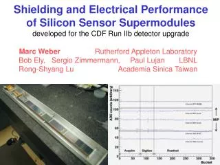
Multi-chip-carrier/hybrid • carries readout chips and passive components (resistors and capacitors • distributes power and control signals to chips; routes data signals out • filters sensor bias voltage • Typically have 4 conductor layers separated by dielectric/insulation layers Example: ceramic BeO hybrid for the CDF detector Size: 38 mm x 20 mm x 0.38 mm
4-chip hybrid: top layer Package efficiency: 31%; 30 passive components; material: 0.18% rad. length; no technical problems; yield on 117 hybrids: 90%(after burn-in)
want low-Z material and small feature size and thickness • (minimize multiple scattering) • good heat conduction to cooling tubes • reliability/ high yield • good electrical performance Critical parameters for hybrids
Packaging 3D packaging Cell phone, Digital camera, PDA, Web access, Outlook “Packaging is what makes your cell phone small” How to stack sensors; MCMs; chips; CF support; cables and cooling while connecting them electrically, thermally and mechanically ?
Technological challenges: Pixel detector • innovative packaging of sensor/chips/support structure/cooling - sophisticated, crowded flex-hybrid - carbon-carbon support structures - bump-bonding of chips to sensors - direct cooling of chips • Global and local support structures: stiff; lightweight; precise; “zero” thermal expansion
Technological challenges: Pixel detector • Bump-bonding of chips to sensors: pitch of only 50 μm (commercial pitches 200 μm)
Packaging solution for SCT Still very compact - flex-hybrid with connectors - separate optical readout for each module - separate power for each module - cooling pipes not integrated to structure
Radiation-hard sensors • Radiation induced leakage current independent of impurities; every 7C of temperature reduction halves current • cool sensors to -25C (SCT = -7C) • “type inversion” from n to p-bulk increased depletion voltage oxygenated silicon helps (for protons); n+-in-n-bulk or n+-in-p-bulk helps • Charge trapping the most dangerous effect at high fluences collect electrons rather than holes reduce drift distances
Strong candidate for inner layer: 3D pixels • 3D pixel proposed by Sherwood Parker in 1985 • vertical electrodes; lateral drift; shorter drift times; much smaller depletion voltage • Difficulty was non-standard via process; meanwhile much progress in hole etching; many groups; simplified designs see talk of Sabina R. (ITC-irst) 3D planar
Signal loss vs. fluence see C. da Via’s talk at STD6 “Hiroshima” conference 3D pixels perform by far the best
Large Hadron Collider: the world’s most powerful accelerator 7 TeV protons vs. 7 TeV protons; 27 km circumference 7 x the energy and 100 x the luminosity of the Tevatron ATLAS detector
ATLAS detector • Huge multi-purpose detector; 46 m long; diameter 22 m; weight 7000 t • Tracking system much smaller; 7 m long; diameter 2.3 m; 2 T field
ATLAS Silicon Tracker 5.6 m 2 m 1 m 1.6 m 17 thousand silicon sensors (60 m2 ) 6 M silicon strips (80 m x 12.8 cm) 80 M pixels (50 m x 400 m) 40 MHz event rate; > 50 kW power
What’s charged particle tracking ? • Measure (many) space points/hits of charged particles • Sort out the mess and reconstruct particle tracks Difficulty is: - not to get confused - achieve track position resolution of 5-10 m 1 billion collisions/sec …it’s not easy ! Up to 1000 tracks
How does it look in real life ? SCT Detector • 4 barrel layers at 30, 37, 45, 52 cm radius and 9 discs (each end) • 60 m2 of silicon; 6 M strips; typical power consumption 50 kW • Precision carbon fiber support cylinder carries modules, cables, optical fiber, and cooling tubes • Evaporative cooling system based on C3F8 (same for pixel detector) Barrel 6 at CERN
Why tracking at LHC is tough ? • Too many particles in too short a time - 1000 particles / bunch collision - too short: collisions every 25 ns • Too short need fast detectors and electronics; power! • Too many particles - need high resolution detectors with millions of channels - detectors suffer from radiation damage to date this requires silicon detectors
Example Need many channels to resolve multi-track patterns Expect 30-60 M strips and >100 M pixels
Extreme radiation levels ! • Radiation levels vary from 1 to 50 MRad in tracker volume - less radiation at larger radii; more close to beam pipe - more radiation in forward regions • Fluences vary from to 1013 to 1015 particles/cm2 • Vicious circle: need silicon sensors for resolution and radiation hardness cooling (sensors and electronics) more material even more secondary particles etc. Don’t win a beauty contest in this environment, but detectors are still very good !
Extreme radiation levels ! Plots show radiation dose and fluence per high luminosity LHC year for ATLAS(assuming 107 s of collisions; source: ATL-Gen-2005-001) Fluence [1 MeV eq. neutrons/cm2] Radiation dose [Gray/year] • “Uniform thermal neutron gas” Put your cell phone into ATLAS ! • It stops working after 1 s to 1 min. • Neutrons are everywhere and cannot easily be suppressed
LHC first years: 1033 cm-2s-1 LHC in 2008 ?? : 1032 cm-2s-1 The Boring masks the Interesting HZZ ee + minimum bias events (MH= 300 GeV) LHC: 1034 cm-2s-1 SLHC: 1035 cm-2s-1
Why are silicon detectors so popular ? • Start from a large signal good resolution; big enough for electronics • Signal formation is fast • Radiation-hardness • SiO2 is a good dielectric • Ride on technological progress of Microelectronics industry extreme control over impurities; very small feature size; packaging technology • Scientist and engineers developed many new concepts over the last two decades
Technologies come and go Random examples are • Bubble chamber
Technologies come and go Steam engines
Silicon detectors are not yet going! Future detectors are being designed and will be • Larger:200-2000 m2 • More channels:Giga pixels • Thinner:20 m • Less noise • Better resolution Your next digital camera will be better and cheaper as well