Download
1 / 12
150 likes | 561 Views
6.772/SMA5111 - Compound Semiconductors. Supplement 1 - Semiconductor Physics Review - Outline. The Fermi function and the Fermi level The occupancy of semiconductor energy levels Effective density of states Conduction and valence band density of states 1. General 2. Parabolic bands

E N D
6.772/SMA5111 - Compound Semiconductors Supplement 1 - Semiconductor Physics Review - Outline The Fermi function and the Fermi level The occupancy of semiconductor energy levels Effective density of states Conduction and valence band density of states 1. General 2. Parabolic bands Quasi Fermi levels The concept and definition Examples of application 1. Uniform electric field on uniform sample 2. Forward biased p-n junction 3. Graded composition p-type heterostructure 4. Band edge gradients as effective forces for carrier drift Refs: R. F. Pierret, Semiconductor Fundamentals 2nd. Ed., (Vol. 1 of the Modular Series on Solid State Devices, Addison-Wesley, 1988); TK7871.85.P485; ISBN 0-201-12295-2. S. M. Sze, Physics of Semiconductor Devices (see course bibliography) Appendix C in Fonstad (handed out earlier; on course web site) C. G. Fonstad, 2/03 Supplement 1- Slide 1
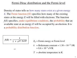
Fermi level and quasi-Fermi Levels - review of key points Fermi level: In thermal equilibrium the probability of finding an energy level at E occupied is given by the Fermi function, f(E): where Ef is the Fermi energy, or level. In thermal equilibrium Ef is constant and not a function of position. The Fermi function has the following useful properties: These relationships tell us that the population of electrons decreases exponentially with energy at energies much more than kT above the Fermi level, and similarly that the population of holes (empty electron states) decreases exponentially with energy when more than kT below the Fermi level. C. G. Fonstad, 2/03 Supplement 1- Slide 2
A final set of useful Fermi function facts are the values of f(E) in the limit of T = 0 K: Effective densities of states: we can define an effective density of states for the conduction band, Nc, as and an effective density of states for the valence band, Nv, as where ρ(E) is the electron density of states in the semiconductor. C. G. Fonstad, 2/03 Supplement 1- Slide 3
If the energy bands are parabolic, i.e., when the density of states depends quadraticly on the energy away from the band edge, we find simple relationships between the densities of states and the effective masses: When (Ec-Ef)>>kT, we can write the thermal equilibrium electronconcentration in terms of effective density of states of the conductionband and the separation between the Fermi level and the conductionband edge, Ec, as: Similarly when (Ef-Ev)>>kT we can write: Note: In homogeneous material Nc, and Nv do not depend on x. C. G. Fonstad, 2/03 Supplement 1- Slide 4
Quasi-Fermi levels: When a semiconductor is not in thermal equilibrium, it is still very likely that the electron population is at equilibrium within the conduction band energy levels, and the hole population is at equilibrium with the energy levels in the valence band. That is to say, the population on electrons is distributed in the conduction band states with the Boltzman factor: Here Efn is the effective, or quasi-, Fermi level for electrons. Similarly, there is a quasi-Fermi level for holes, Efp, and the holes aredistributed in the valence band states as: The quasi-Fermi levels for electrons and holes, Efn and Efp, are not in general equal. To find them we usually begin with n(x) and p(x), and write them in terms of the conduction and valence band densities of states and the quasi-Fermi levels: C. G. Fonstad, 2/03 Supplement 1- Slide 5
Quasi-Fermi levels, cont.: A very important finding involving quasi-Fermi levels is that we can write the electron and hole currents in terms of the gradients of the respective quasi-Fermi levels, at least in the low field limit where drift mobility is a valid concept. We find: and Examples: A. Uniformly doped n-type semiconductor with uniform E-field At low to moderate E-fields, the populations are not disturbed from their equilibrium values, and we have As expected, the currents are the respective drift currents. C. G. Fonstad, 2/03 Supplement 1- Slide 6
B. P-side of forward biased n+-p junction, long-base limit: Diode diffusion theory gives us n(x) on the p-side*: When vAB >> kT, and x is not many Le, we can approximate n(x) as : from which we find: We see that Efn(x) is qvAB higher than the equilibrium Fermi level, Efo, at the edge of the depletion region on the p-side, and decreases linearly going away from the junction. Farther away from the junction, where x is many Le, n(x) approaches nop, and Efn(x) approaches Efo. Finally, notice that for low-level injection, p(x) ≈ ppo , and Efp ≈ Efo . C. G. Fonstad, 2/03 Supplement 1- Slide 7
Quasi-Fermi levels - Illustrating examples A and B Figure C-8 from Fonstad, Microelectronic Devices and Circuits with quasi-Fermi levels added: C. G. Fonstad, 2/03 Supplement 1- Slide 8
C. Graded composition p-type heterostructure with uniform low level electron injection. Assume the grading is from Eg1, X1 @ x = 0, and Eg1, X1 @ x = L. In thermal equilibrium the Fermi level, Efo, is flat, and the valence band edge is flat: whereas the conduction band edge slopes: With low-level electron injection, n(x) ≈ n’ (>>npo): Hole population is changed insignificantly, and Efp(x) ≈ Efo Electron population is now n’, and so Using this to get Je(x), we find From this we see that the band gap grading acts like an effective electric field acting on the electrons (but not on the holes)! C. G. Fonstad, 2/03 Supplement 1- Slide 9
Quasi-Fermi levels - Illustrating example C C. G. Fonstad, 2/03 Supplement 1- Slide 10
D. General meaning of band-edge gradings In general we can write the electron quasi-Fermi level as: and thus in general we can write the electron current as: With low-level electron injection, n(x) ≈ n’ (>>npo): Hole population is changed insignificantly, and Efp(x) ≈ Efo Electron population is now n’, and so [Note: In getting this we have used the Einstien relation and definitionof conductivity: ] From our final result we see that the gradient in the conduction band edge is the force leading to electron drift, while the gradient in the carrier and density of states concentrations are the diffusion force. Discussion continued for holes on next foil. C. G. Fonstad, 2/03 Supplement 1- Slide 11
D. cont. We obtain the corresponding result for holes if we similarly substitute valence band quantities for conduction band quantities. Begin with: and thus Now we see that the gradient in the valence band edge is the force leading to hole drift, while the gradient in the carrier and density of states concentrations are the diffusion force. Summarizing, the conduction and valence band-edge gradients can be viewed as effective electric fields for electrons and holes, respectively: C. G. Fonstad, 2/03 Supplement 1- Slide 12