Download
1 / 43
430 likes | 578 Views
Ductile Regime Nano-Machining : Comparison of Numerical and Experimental Results during Scratching of Silicon and Silicon Carbide. Dr. John A Patten, Western Michigan University, Manufacturing Engineering. AGENDA. Introduction Research Background

E N D
Ductile Regime Nano-Machining:Comparison of Numerical and Experimental Results during Scratching of Silicon and Silicon Carbide Dr. John A Patten, Western Michigan University, Manufacturing Engineering
AGENDA • Introduction • Research Background • Ductile Regime Machining of Silicon and Silicon Carbide • Determination of Ductile to Brittle Transition (DBT) depth for Chemically Vapor Deposited (CVD) Silicon Carbide (SiC) • Single Point Diamond Turning (SPDT) of CVD coated SiC • Determination of DBT depth for Quartz • Conclusion • Future Work
INTRODUCTION Defining important terms: • High Pressure Phase Transformation • Nano – Machining • Ductile Regime • Ductile to Brittle Transition Depth
Overview of presentation • Introduction to HPPT in ceramics • Examples of HPPT in ceramics • Scratching experiments on silicon • Scratching experiments on silicon carbide • Simulations of scratching experiments • Silicon • Silicon Carbide • Machining of Silicon Carbide
Silicon Simulation result Pressures at the tool-workpiece interface are at least 12GPa or higher. 12 GPa is the hardness of the this Silicon material.
Materials • Single Crystal (Cree and SiCrystal) • 6H • 4H • 3C • Polycrystalline • CoorsTek: 6H, Beta • CVD: 6H, Beta • CoorsTek • Poco Graphite
Basics of HPPT and importance in Ceramics • Definition of HPPT and relation to hardness of the material. • D-B-T depth in ceramics. • Importance of HPPT in ceramic manufacturing
HPPT Theoretical/Exp. Analysis • Ab initio • Theoretical HPPT pressure: 65 GPa • Possible 3C to 6H HPPT
HPPT Theoretical Analsis (cont) • Molecular Dynamics • Scratching/Machining-Amorphization • Very nigh speeds (100-400 m/s) • Thermal softening effects significant • No evidence of dislocations • Nanoindentation (3C & 6H) • Plastic behavior related to phase transition • HPPT (100-150 GPa) • Critical Pressure for onset of plastic deformation: 45 GPa • Scratch Hardness < Indentation Hardness • Suggesting influence of shear • Shear stress tends to lower transformation pressure
Experimental Analysis • DAC • 3C fourfold coordinate to sixfold • metallic at 100 GPa, 20% volume reduction • 6H No High Pressure data above 95 GPa • Precursor to HPPT at 95 GPa • R-DAC: amorphization? • Shock Compression (Also substantial temperature rise due to high strain rates) • 6H PT at 105 GPa, with 15% volume reduction, suggested to probably be sixfold coordinated metallic structure
Experiments (cont.) • Nanoindentation • 6H: amorphization/ no amorphization • Scratching • 6H: amorphization • Machining-SPDT: • S.C. & Poly: 6H: • amorphous remnant/debris - chips
Ductile Response of SiC @ RT • Nanoindentation 50 mN (no cracking and no chipping) Figure. SEM micrographs of indented SiC
Ductile Response of SiC @ RT (cont) • Scratching Ductile
Ductile Response of SiC @ RT (cont) • Scratching • 4H scratch Ductile Scratch: 25 mN, 0.3 mm/s With IR Laser Heating 1000 mA
Scratching SiC 1: 25 mN, 0.3 mm/s 2: 1000 mA IR laser 3: Speed < 0.3 mm/s
Determination of D-B-T depth Optical image of a typical D-B-T in a scratch
DETERMINATION OF DBT DEPTH FOR CVD coated SiC Wyko image of scratch of Coors Tek sample using 5 µm diamond stylus Wyko image of scratch of Poco Graphite sample using 5 µm diamond stylus
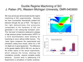
DBT depth = 400 nm DETERMINATION OF DBT DEPTH FOR CVD coated SiC DBT depth for Coors Tek Sample: SEM of the used 12.5 micron diamond stylus for Coors Tek sample Wyko image for DBT depth of Coors Tek sample using 12.5 µm stylus Force and AE plot for DBT depth of Coors Tek sample using 12.5 µm stylus
DBT depth = 550 nm DBT depth DETERMINATION OF DBT DEPTH FOR CVD coated SiC DBT depth for Poco Graphite Sample: SEM of the used 12.5 micron diamond stylus for Poco Graphite sample Wyko image for DBT depth of Poco Graphite sample using 12.5 µm stylus Force and AE plot for DBT depth of Poco Graphite sample using 12.5 µm stylus
DETERMINATION OF DBT DEPTH FOR CVD coated SiC SEM of the failed tool edge used for inclined plane experiment Wyko image of scratch on Poco Graphite using inclined plane experiment Force plot of scratch on Poco Graphite using inclined plane experiment
Result from simulations of silicon carbide • Thrust force values show good agreement. • Forces seem to be converging at high COF.
Summary of simulations and conclusion • Summary of 3-D scratching simulations • Si simulations show simulation thrust force is lower than experimental value. • Why? • SiC simulations show thrust forces in good agreement with the experiment. (even though depths are different?_ • SiC simulations show cutting forces that are not in very good agreement with the experiment. • Why? • 3-D scratching work shows encouraging results • initial attempts at simulations of ductile behavior of ceramic materials • nanometer depths, • below the DBT depth of these nominally brittle materials.
Ductile Response of SiC @ RT Machining (SPDT) • Machining
MD Simulation – 3C SiC • Alice Noreyan, Univ. of Toledo
Origin of Ductile Response • High Temperatures > 1000 C • Dislocation plasticity • Low Temperature • Amorphous • Phase Transformation? • Back Transformation ? • HPPT • In-situ detection • R-DAC, nanoindentation: micro-Raman, x-ray, IR laser
Post Process Analysis • DAC/R-DAC • Incomplete analysis • Nanoindentation: Ductile response at low loads • Amorphization not consistent • Scratching: Ductile response at low loads • Amorphorization • Machining: Ductile response at low depths • Amorphization
Post Process Characterization • Optical and SEM • TEM • Raman and micro Raman (UV) • Crystal IP Amorphous ? HPPT
Ductility=Amorphous (HP)PT • Machining • The ductile chips are amorphous • Crystal to amorphous phase transformation
Hardness~HPPT • Ductility ~ f[HPPT @ RT]? • Hardness: 26-36 GPa, up to 80 GPa • Athermal region similar to Si & Ge
Amorphization • Recrystallization? • DAC • Indents • Machining Chips • Additional work needs to be done • Time and temperature factors • Evaluate crystal structure immediately • Raman and TEM of Scratches and Indents • Radiation heating effects
Other Effects • Recrystallization • Surface provides “seed” for nucleation and grain growth • Chips/Debris – no seed mechanism? • Shear contribution to HPPT • High in Machining, Scratching • Low in indentation, DAC • Possibly high in R-DAC
Ductile to Brittle Transition (DBT): Silicon Carbide • Plastic-Ductile Deformation • Critical Depths, Critical Depth of cut, Force • Indents: 50-80 mN • Scratches: 40-120 nm • Machining: 50-100 nm • CVD SiC: 400-550 nm
Acknowledgements • NSF for the research grants (DMR and DMI) • University Partners: UW-P, NCSU, UT-K, UNC-C, TTU, PSU, • Andy Grevstad and Third Wave Systems for software and funding support. • Dr Guichelaar for equipment at the Tribology lab. • Lei Dong at University of North Carolina at Charlotte Si work) • Biswarup Bhattacharya (WMU) for CVD coated SiC work. • Jerry Jacob (WMU) for simulations • ORNL: HTML, Peter Blau, et al. • Hisham Abdel-Aal, UW-P, analysis support
Future • In situ Characterization • R-DAC with high pressures and large shear • Nanoindentation with Raman and x-ray • Post Process Characterization • TEM • Processing (reduce forces, reduce tool wear) • IR laser assisted machining • Fluid assisted cutting
Questions and comments Contact: john.patten@wmich.edu